EVAL-ADUC831QSZ Analog Devices Inc, EVAL-ADUC831QSZ Datasheet
EVAL-ADUC831QSZ
Specifications of EVAL-ADUC831QSZ
EVAL-ADUC831QS


Related parts for EVAL-ADUC831QSZ


EVAL-ADUC831QSZ Summary of contents
Page 1
FEATURES ANALOG I/O 8-Channel, 247 kSPS 12-Bit ADC DC Performance: 1 LSB INL AC Performance SNR DMA Controller for High Speed ADC-to-RAM Capture 2 12-Bit (Monotonic) Voltage Output DACs Dual Output PWM/ - DACs On-Chip Temperature Sensor Function ...
Page 2
ADuC831 TABLE OF CONTENTS FEATURES . . . . . . . . . . . . . . . . . . . . . . . . . . . . . . . . . . 1 ...
Page 3
SPECIFICATIONS all specifications T Parameter ADC CHANNEL SPECIFICATIONS ACCURACY Resolution Integral Nonlinearity Differential Nonlinearity 4 Integral Nonlinearity 4 Differential Nonlinearity Code Distribution CALIBRATED ENDPOINT ERRORS Offset Error Offset Error Match Gain Error Gain Error Match ...
Page 4
ADuC831 SPECIFICATIONS (continued) Parameter DAC CHANNEL SPECIFICATIONS Internal Buffer Disabled 10 DC ACCURACY Resolution Relative Accuracy 11 Differential Nonlinearity Offset Error Gain Error 4 Gain Error Mismatch ANALOG OUTPUTS Voltage Range_0 REFERENCE INPUT/OUTPUT 14 REFERENCE OUTPUT Output Voltage (V ) ...
Page 5
Parameter 4 SCLOCK and RESET Only (Schmitt-Triggered Inputs T– V – T– CRYSTAL OSCILLATOR Logic Inputs, XTAL1 Only V , Input Low Voltage INL V , Input High Voltage INH XTAL1 Input Capacitance XTAL2 Output ...
Page 6
ADuC831 SPECIFICATIONS (continued) Parameter 19, 20 POWER REQUIREMENTS Power Supply Voltages AV /DV to AGND DD DD Power Supply Currents Normal Mode DV Current DD AV Current DD DV Current DD AV Current DD Power Supply Currents Idle Mode DV ...
Page 7
... ADuC831BCP –40°C to +85°C EVAL-ADuC831QS EVAL-ADuC831QSP CAUTION ESD (electrostatic discharge) sensitive device. Electrostatic charges as high as 4000 V readily accumulate on the human body and test equipment and can discharge without detection. Although the ADuC831 features proprietary ESD protection circuitry, permanent damage may occur on devices subjected to high energy electrostatic discharges ...
Page 8
ADuC831 P1.0/ADC0/T2 1 PIN 1 2 IDENTIFIER P1.1/ADC1/T2EX 3 P1.2/ADC2 4 P1.3/ADC3 AGND 6 ADuC831 52-LEAD PQFP C 7 TOP VIEW REF (Not to ...
Page 9
Mnemonic Type Function DV P Digital Positive Supply Voltage Nominal Analog Positive Supply Voltage Nominal DD Decoupling Input for On-Chip Reference. Connect 0.1 µF between this pin ...
Page 10
ADuC831 Mnemonic Type Function PSEN O Program Store Enable, Logic Output. This output is a control signal that enables the external program memory to the bus during external fetch operations active every six oscillator periods except during external ...
Page 11
The typical performance plots presented in this section illustrate typical performance of the ADuC831 under various operating conditions. TPC 1 and TPC 2 below show typical ADC Integral Nonlinearity (INL) errors from ADC code 0 to code 4095 at 5 ...
Page 12
ADuC831 1.0 0.8 0.6 0.4 0.2 0 –0.2 –0.4 –0.6 –0.8 –1.0 0 511 1023 1535 2047 2559 ADC CODES TPC 5. Typical DNL Error, V 1.0 0.8 0.6 0.4 0.2 0 –0.2 –0.4 –0.6 –0.8 –1.0 0 511 1023 ...
Page 13
FREQUENCY – kHz TPC 11. Dynamic Performance –20 –40 –60 –80 –100 –120 –140 –160 FREQUENCY ...
Page 14
ADuC831 MEMORY ORGANIZATION The ADuC831 contains four different memory blocks: • 62 kBytes of On-Chip Flash/EE Program Memory • 4 kBytes of On-Chip Flash/EE Data Memory • 256 Bytes of General-Purpose RAM • 2 kBytes of Internal XRAM Flash/EE Program ...
Page 15
External Data Memory (External XRAM) Just like a standard 8051 compatible core, the ADuC831 can access external data memory using a MOVX instruction. The MOVX instruction automatically outputs the various control strobes required to access the data memory. The ADuC831, ...
Page 16
ADuC831 Data Pointer (DPTR) The Data Pointer is made up of three 8-bit registers, named DPP (page byte), DPH (high byte) and DPL (low byte). These are used to provide memory addresses for internal and external code access and external ...
Page 17
SPECIAL FUNCTION REGISTERS All registers except the program counter and the four general- purpose register banks, reside in the special function register (SFR) area. The SFR registers include control, configuration, and data registers that provide an interface between the CPU ...
Page 18
ADuC831 ADC CIRCUIT INFORMATION General Overview The ADC conversion block incorporates a fast, 8-channel, 12-bit, single supply ADC. This block provides the user with multichannel mux, track/hold, on-chip reference, calibration features, and ADC. All components in this block are easily ...
Page 19
ADCCON1 – (ADC Control SFR #1) The ADCCON1 register controls conversion and acquisition times, hardware conversion modes and power-down modes as detailed below. SFR Address: EFH SFR Power-On Default Value: 00H Bit Addressable: NO Bit Name Description ADCCON1.7 MD1 The ...
Page 20
ADuC831 ADCCON2 – (ADC Control SFR #2) The ADCCON2 register controls ADC channel selection and conversion modes as detailed below. SFR Address: D8H SFR Power-On Default Value: 00H Bit Addressable: YES Name Description Bit ADCCON2.7 ADCI The ADC interrupt bit ...
Page 21
ADCCON3 – (ADC Control SFR #3) The ADCCON3 register controls the operation of various calibra- tion modes as well as giving an indication of ADC busy status. SFR Address: F5H SFR Power-On Default Value: 00H Bit Addressable: NO Bit Name ...
Page 22
ADuC831 Driving the A/D Converter The ADC incorporates a successive approximation (SAR) archi- tecture involving a charge-sampled input stage. Figure 9 shows the equivalent circuit of the analog input section. Each ADC conversion is divided into two distinct phases as ...
Page 23
Keep in mind that the ADC’s transfer function any signal range lost to amplifier saturation near ground will impact dynamic range. Though the op amps in Table VI are capable of delivering output signals very closely ...
Page 24
ADuC831 Configuring the ADC The ADuC831’s successive approximation ADC is driven by a divided down version of the master clock. To ensure adequate ADC operation, this ADC clock must be between 400 kHz and 6 MHz, and optimum performance is ...
Page 25
The DMA logic operates from the ADC clock and uses pipelining to perform the ADC conversions and access the external memory at the same time. The time it takes to perform one ADC conversion is called a DMA cycle. The ...
Page 26
ADuC831 INITIATING CALIBRATION IN CODE When calibrating the ADC, using ADCCON1 the ADC should be set up into the configuration in which it will be used. The ADCCON3 register can then be used to set the device up and calibrate ...
Page 27
NONVOLATILE FLASH/EE MEMORY Flash/EE Memory Overview The ADuC831 incorporates Flash/EE memory technology on-chip to provide the user with nonvolatile, in-circuit reprogrammable code, and data memory space. Flash/EE memory is a relatively recent type of nonvolatile memory technology and is based ...
Page 28
ADuC831 Using the Flash/EE Program Memory The 62 kByte Flash/EE program memory array is mapped into the lower 62 kBytes of the 64 kBytes program space addressable by the ADuC831, and is used to hold user code in typical applications. ...
Page 29
USING THE FLASH/EE DATA MEMORY The 4 kBytes of Flash/EE data memory is configured as 1024 pages, each of four bytes. As with the other ADuC831 peripherals, the interface to this memory space is via a group of registers mapped ...
Page 30
ADuC831 Example: Programming the Flash/EE Data Memory A user wishes to program F3H into the second byte on Page 03H of the Flash/EE data memory space while preserving the other three bytes already in this page. A typical program of ...
Page 31
ADuC831 Configuration SFR (CFG831) The CFG831 SFR contains the necessary bits to configure the internal XRAM, EPROM controller, PWM output selection and frequency, DAC buffer, and the extended SP. By default it configures the user into 8051 mode, i.e., extended ...
Page 32
ADuC831 USER INTERFACE TO OTHER ON-CHIP ADuC831 PERIPHERALS The following section gives a brief overview of the various peripherals also available on-chip. A summary of the SFRs used to control and configure these peripherals is also given. DAC The ADuC831 ...
Page 33
Using the DAC The on-chip DAC architecture consists of a resistor string DAC followed by an output buffer amplifier, the functional equivalent of which is illustrated in Figure 21. Details of the actual DAC architecture can be found in U.S. ...
Page 34
ADuC831 3 DAC LOADED WITH 0FFFH 2 1 DAC LOADED WITH 0000H SOURCE/SINK CURRENT – mA Figure 24. Source and Sink Current Capability with REF DD To reduce the effects of ...
Page 35
PULSEWIDTH MODULATOR (PWM) The PWM on the ADuC831 is highly flexible PWM offering programmable resolution and input clock, and can be config- ured for any one of six different modes of operation. Two of these modes allow the PWM to ...
Page 36
ADuC831 PWM MODES OF OPERATION MODE 0: PWM Disabled The PWM is disabled, allowing P2.6 and P2 used as normal. MODE 1: Single Variable Resolution PWM In Mode 1, both the pulse length and the cycle time (period) ...
Page 37
MODE 4: Dual NRZ 16-Bit - DAC Mode 4 provides a high speed PWM output similar to that DAC. Typically, this mode will be used with the PWM clock equal to 16 MHz. In this mode P2.6 ...
Page 38
ADuC831 SERIAL PERIPHERAL INTERFACE The ADuC831 integrates a complete hardware Serial Peripheral Interface (SPI) on-chip. SPI is an industry standard synchronous serial interface that allows eight bits of data to be synchronously transmitted and received simultaneously, i.e., full duplex. It ...
Page 39
SPIDAT SPI Data Register Function The SPIDAT SFR is written by the user to transmit data over the SPI interface or read by user code to read data just received by the SPI interface. SFR Address F7H Power-On Default Value ...
Page 40
ADuC831 COMPATIBLE INTERFACE The ADuC831 supports a fully licensed interface is implemented as a full hardware slave and software master. SDATA is the data I/O pin and SCLOCK is the serial clock. These two ...
Page 41
The main features of the MicroConverter I • Only two bus lines are required; a serial data line (SDATA) and a serial clock line (SCLOCK). • master can communicate with multiple slave devices. Because each slave ...
Page 42
ADuC831 DUAL DATA POINTER The ADuC831 incorporates two data pointers. The second data pointer is a shadow data pointer and is selected via the data pointer control SFR (DPCON). DPCON also includes some nice features such as automatic hardware post-increment ...
Page 43
POWER SUPPLY MONITOR As its name suggests, the Power Supply Monitor, once enabled, monitors the DV supply on the ADuC831. It will indicate DD when any of the supply pins drops below one of four user- selectable voltage trip points, ...
Page 44
ADuC831 WATCHDOG TIMER The purpose of the watchdog timer is to generate a device reset or interrupt within a reasonable amount of time if the ADuC831 enters an erroneous state, possibly due to a program- ming error or electrical noise. ...
Page 45
TIME INTERVAL COUNTER (TIC) A time interval counter is provided on-chip for counting longer intervals than the standard 8051 compatible timers are capable of. The TIC is capable of timeout intervals ranging from 1/128 second to 255 hours. Furthermore, this ...
Page 46
ADuC831 INTVAL User Time Interval Select Register Function User code writes the required time interval to this register. When the 8-bit interval counter is equal to the time interval value loaded in the INTVAL SFR, the TII bit (TIMECON.2) is ...
Page 47
COMPATIBLE ON-CHIP PERIPHERALS This section gives a brief overview of the various secondary peripheral circuits that are also available to the user on-chip. These remaining functions are mostly 8052 compatible (with a few additional features) and are controlled via ...
Page 48
ADuC831 In general-purpose I/O port mode, Port 2 pins that have 1s written to them are pulled high by the internal pull-ups (Figure 39) and, in that state, they can be used as inputs. As inputs, Port 2 pins being ...
Page 49
SPE = ENABLE) 2 HARDWARE I C (SLAVE ONLY) 50ns GLITCH SFR REJECTION FILTER BITS MCO I2CM Figure 42. SCLOCK Pin I/O Functional Equivalent Mode DV SPE = 1 (SPI ENABLE) Q1 ...
Page 50
ADuC831 Timers/Counters The ADuC831 has three 16-bit Timer/Counters: Timer 0, Timer 1, and Timer 2. The Timer/Counter hardware has been included on-chip to relieve the processor core of the overhead inherent in implementing Timer/Counter functionality in soft- ware. Each Timer/Counter ...
Page 51
TCON Timer/Counter 0 and 1 Control Register SFR Address 88H Power-On Default Value 00H Bit Addressable Yes Bit Name Description 7 TF1 Timer 1 Overflow Flag. Set by hardware on a Timer/Counter 1 overflow. Cleared by hardware when the Program ...
Page 52
ADuC831 TIMER/COUNTER 0 AND 1 OPERATING MODES The following paragraphs describe the operating modes for Timer/Counters 0 and 1. Unless otherwise noted, it should be assumed that these modes of operation are the same for Timer 0 as for Timer ...
Page 53
T2CON Timer/Counter 2 Control Register SFR Address C8H Power-On Default Value 00H Bit Addressable Yes Bit Name Description 7 TF2 Timer 2 Overflow Flag. Set by hardware on a Timer 2 overflow. TF2 will not be set when either RCLK ...
Page 54
ADuC831 Timer/Counter Operation Modes The following paragraphs describe the operating modes for Timer/Counter 2. The operating modes are selected by bits in the T2CON SFR as shown in Table XXII. Table XXII. T2CON Operating Modes RCLK (or) TCLK CAP2 TR2 ...
Page 55
UART SERIAL INTERFACE The serial port is full duplex, meaning it can transmit and receive simultaneously also receive-buffered, meaning it can com- mence reception of a second byte before a previously received byte has been read from the ...
Page 56
ADuC831 Mode 0: 8-Bit Shift Register Mode Mode 0 is selected by clearing both the SM0 and SM1 bits in the SFR SCON. Serial data enters and exits through RxD. TxD outputs the shift clock. Eight data bits are transmitted ...
Page 57
Timer 1 Generated Baud Rates When Timer 1 is used as the baud rate generator, the baud rates in Modes 1 and 3 are determined by the Timer 1 overflow rate and the value of SMOD as follows: Modes 1 ...
Page 58
ADuC831 Timer 3 Generated Baud Rates The high integer dividers in a UART block mean that high speed baud rates are not always possible using some particular crystals. For example, using a 12 MHz crystal, a baud rate of 115200 ...
Page 59
INTERRUPT SYSTEM The ADuC831 provides a total of nine interrupt sources with two priority levels. The control and configuration of the interrupt system is carried out through three Interrupt-related SFRs. IE Interrupt Enable Register IP Interrupt Priority Register IEIP2 Secondary ...
Page 60
ADuC831 Interrupt Priority The Interrupt Enable registers are written by the user to enable individual interrupt sources, while the Interrupt Priority registers allow the user to select one of two priority levels for each interrupt. An interrupt of a high ...
Page 61
Port 0 (P0) serves as a multiplexed address/data bus. It emits the low byte of the program counter (PCL address, and then goes into ...
Page 62
ADuC831 As an alternative to providing two separate power supplies, the user can help keep AV quiet by placing a small series resistor DD and/or ferrite bead between it and separately to ground. An example of this ...
Page 63
TYP DV DD 128ms TYP 128ms TYP 1.0V TYP INTERNAL CORE RESET Figure 62. Internal POR Operation Grounding and Board Layout Recommendations As with all high resolution data converters, special attention must be paid to grounding and PC board ...
Page 64
ADuC831 ANALOG INPUT VREF OUTPUT DAC OUTPUT C1+ V+ C1– C2+ C2– V– T2OUT R2IN Figure 64. Example ADuC831 System (PQFP Package) Note that PSEN is normally an output (as described in the External Memory Interface section) and is sampled ...
Page 65
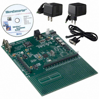
... The QuickStart Development System is an entry-level, low cost development tool suite supporting the ADuC831. The system consists of the following PC-based (Windows hardware and software development tools. Hardware: ADuC831 Evaluation Board and Serial Port Programming Cable. Software: ASPIRE Integrated Development Environment. Incorporates 8051 assembler and serial port debugger ...
Page 66
ADuC831 TIMING SPECIFICATIONS Parameter CLOCK INPUT (External Clock Driven XTAL1) t XTAL1 Period CK t XTAL1 Width Low CKL t XTAL1 Width High CKH t XTAL1 Rise Time CKR t XTAL1 Fall Time CKF 4 t ADuC831 ...
Page 67
Parameter EXTERNAL PROGRAM MEMORY READ CYCLE t ALE Pulsewidth LHLL t Address Valid to ALE Low AVLL t Address Hold after ALE Low LLAX t ALE Low to Valid Instruction In LLIV ALE Low to PSEN Low t LLPL PSEN ...
Page 68
ADuC831 Parameter EXTERNAL DATA MEMORY READ CYCLE RD Pulsewidth t RLRH t Address Valid after ALE Low AVLL t Address Hold after ALE Low LLAX RD Low to Valid Data In t RLDV Data and Address Hold after RD t ...
Page 69
Parameter EXTERNAL DATA MEMORY WRITE CYCLE WR Pulsewidth t WLWH t Address Valid after ALE Low AVLL t Address Hold after ALE Low LLAX ALE Low Low t LLWL Address Valid Low ...
Page 70
ADuC831 Parameter UART TIMING (Shift Register Mode) t Serial Port Clock Cycle Time XLXL t Output Data Setup to Clock QVXH t Input Data Setup to Clock DVXH t Input Data Hold after Clock XHDX t Output Data Hold after ...
Page 71
Parameter COMPATIBLE INTERFACE TIMING t SCLOCK Low Pulsewidth L t SCLOCK High Pulsewidth H t Start Condition Hold Time SHD t Data Setup Time DSU t Data Hold Time DHD t Setup Time for Repeated Start RSU ...
Page 72
ADuC831 Parameter SPI MASTER MODE TIMING (CPHA = 1) t SCLOCK Low Pulsewidth SL t SCLOCK High Pulsewidth SH t Data Output Valid after SCLOCK Edge DAV t Data Input Setup Time before SCLOCK Edge DSU t Data Input Hold ...
Page 73
Parameter SPI MASTER MODE TIMING (CPHA = 0) t SCLOCK Low Pulsewidth SL t SCLOCK High Pulsewidth SH t Data Output Valid after SCLOCK Edge DAV t Data Output Setup before SCLOCK Edge DOSU t Data Input Setup Time before ...
Page 74
ADuC831 Parameter SPI SLAVE MODE TIMING (CPHA = SCLOCK Edge SCLOCK Low Pulsewidth SL t SCLOCK High Pulsewidth SH t Data Output Valid after SCLOCK Edge DAV t Data Input Setup Time before SCLOCK ...
Page 75
Parameter SPI SLAVE MODE TIMING (CPHA = SCLOCK Edge SCLOCK Low Pulsewidth SL t SCLOCK High Pulsewidth SH t Data Output Valid after SCLOCK Edge DAV t Data Input Setup Time before SCLOCK Edge ...
Page 76
ADuC831 1.03 0.88 0.73 SEATING PLANE VIEW A 0.23 0.11 BSC SQ PIN 1 INDICATOR 1.00 12 MAX 0.90 0.80 0.25 REF SEATING PLANE OUTLINE DIMENSIONS 52-Lead Plastic Quad Flatpack [MQFP] (S-52) Dimensions shown in millimeters 14.15 13.90 SQ 2.45 ...