EVAL-ADUC831QSZ Analog Devices Inc, EVAL-ADUC831QSZ Datasheet - Page 34
EVAL-ADUC831QSZ
Manufacturer Part Number
EVAL-ADUC831QSZ
Description
KIT DEV FOR ADUC831 QUICK START
Manufacturer
Analog Devices Inc
Series
QuickStart™ Kitr
Type
MCUr
Datasheet
1.EVAL-ADUC831QSZ.pdf
(76 pages)
Specifications of EVAL-ADUC831QSZ
Contents
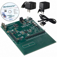
Evaluation Board, Power Supply, Cable, Software and Documentation
Silicon Manufacturer
Analog Devices
Core Architecture
8051
Silicon Core Number
ADuC831
Tool / Board Applications
General Purpose MCU, MPU, DSP, DSC
Mcu Supported Families
ADUC8xx
Development Tool Type
Hardware - Eval/Demo Board
Rohs Compliant
Yes
Lead Free Status / RoHS Status
Lead free / RoHS Compliant
For Use With/related Products
ADuC831
Lead Free Status / Rohs Status
Compliant
Other names
EVAL-ADUC831QS
EVAL-ADUC831QS
EVAL-ADUC831QS


ADuC831
To reduce the effects of the saturation of the output amplifier at
values close to ground and to give reduced offset and gain errors,
the internal buffer can be bypassed. This is done by setting the
DBUF bit in the CFG831 register. This allows a full rail-to-rail
output from the DAC which should then be buffered externally
using a dual supply op-amp in order to get a rail-to-rail output.
This external buffer should be located as near as physically
possible to the DAC output pin on the PCB. Note the unbuffed
mode only works in the 0 to V
Figure 24. Source and Sink Current Capability with
V
REF
= V
3
2
1
0
0
DD
DAC LOADED WITH 0FFFH
DAC LOADED WITH 0000H
= 3 V
SOURCE/SINK CURRENT – mA
5
REF
range.
10
15
–34–
To drive significant loads with the DAC outputs, external buff-
ering may be required (even with the internal buffer enabled),
as illustrated in Figure 25. A list of recommended op-amps is in
Table VI.
The DAC output buffer also features a high-impedance disable
function. In the chip’s default power-on state, both DACs are
disabled, and their outputs are in a high-impedance state (or
“three-state”) where they remain inactive until enabled in software.
This means that if a zero output is desired during power-up or
power-down transient conditions, then a pull-down resistor must
be added to each DAC output. Assuming this resistor is in place,
the DAC outputs will remain at ground potential whenever the
DAC is disabled.
Figure 25. Buffering the DAC Outputs
DAC0
DAC1
ADuC831
REV. 0
Related parts for EVAL-ADUC831QSZ
Image
Part Number
Description
Manufacturer
Datasheet
Request
R


Part Number:
Description:
BOARD EVAL FOR SI270X-A
Manufacturer:
Silicon Laboratories Inc
Datasheet:

Part Number:
Description:
BUCK CONV REF DESIGN KIT IP1201
Manufacturer:
International Rectifier
Datasheet:
Part Number:
Description:
BOARD DEMO SYNC DUAL BUCK CNVTER
Manufacturer:
International Rectifier
Datasheet:
Part Number:
Description:
BOARD DEMO SYNC BUCK CONVETER
Manufacturer:
International Rectifier
Datasheet:

Part Number:
Description:
EVALBOARD/EB Omnidirectional microphone - Analog
Manufacturer:
Analog Devices
Datasheet:
Part Number:
Description:
EVALBOARD/EB Omnidirectional microphone - Analog
Manufacturer:
Analog Devices
Datasheet:


Part Number:
Description:
BOARD EVAL LED DRIVER LT3756
Manufacturer:
Linear Technology
Datasheet:

Part Number:
Description:
BOARD EVAL FOR AD7741/7742
Manufacturer:
Analog Devices Inc
Datasheet:

Part Number:
Description:
±1.7g Dual-Axis IMEMS Accelerometer Evaluation Board
Manufacturer:
Analog Devices Inc
Datasheet:

Part Number:
Description:
IC MULTIPLIER ANALOG 8-SOIC T/R
Manufacturer:
Analog Devices Inc
Datasheet:

Part Number:
Description:
IC ANALOG MULTIPLIER 8-DIP
Manufacturer:
Analog Devices Inc
Datasheet:
Part Number:
Description:
IC ANALOG MULTIPLIER 8-SOIC
Manufacturer:
Analog Devices Inc
Datasheet:
Part Number:
Description:
IC ANALOG MULTIPLIER 8-DIP
Manufacturer:
Analog Devices Inc
Datasheet: