EVAL-ADUC831QSZ Analog Devices Inc, EVAL-ADUC831QSZ Datasheet - Page 32
EVAL-ADUC831QSZ
Manufacturer Part Number
EVAL-ADUC831QSZ
Description
KIT DEV FOR ADUC831 QUICK START
Manufacturer
Analog Devices Inc
Series
QuickStart™ Kitr
Type
MCUr
Datasheet
1.EVAL-ADUC831QSZ.pdf
(76 pages)
Specifications of EVAL-ADUC831QSZ
Contents
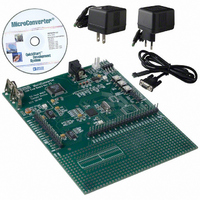
Evaluation Board, Power Supply, Cable, Software and Documentation
Silicon Manufacturer
Analog Devices
Core Architecture
8051
Silicon Core Number
ADuC831
Tool / Board Applications
General Purpose MCU, MPU, DSP, DSC
Mcu Supported Families
ADUC8xx
Development Tool Type
Hardware - Eval/Demo Board
Rohs Compliant
Yes
Lead Free Status / RoHS Status
Lead free / RoHS Compliant
For Use With/related Products
ADuC831
Lead Free Status / Rohs Status
Compliant
Other names
EVAL-ADUC831QS
EVAL-ADUC831QS
EVAL-ADUC831QS


ADuC831
USER INTERFACE TO OTHER ON-CHIP ADuC831
PERIPHERALS
The following section gives a brief overview of the various
peripherals also available on-chip. A summary of the SFRs
used to control and configure these peripherals is also given.
DAC
The ADuC831 incorporates two 12-bit, voltage output DACs
on-chip. Each has a rail-to-rail voltage output buffer capable of
driving 10 kΩ/100 pF. Each has two selectable ranges, 0 V to
V
Each can operate in 12-bit or 8-bit mode. Both DACs share a
control register, DACCON, and four data registers, DAC1H/L,
DACxH/L
Function
SFR Address
Power-On Default Value
Bit Addressable
The 12-bit DAC data should be written into DACxH/L right-justified such that DACxL contains the lower eight bits, and the lower
nibble of DACxH contains the upper four bits.
Bit
7
6
5
4
3
2
1
0
REF
(the internal band gap 2.5 V reference) and 0 V to AV
Name
MODE
RNG1
RNG0
CLR1
CLR0
SYNC
PD1
PD0
The DAC MODE bit sets the overriding operating mode for both DACs.
DAC1 Range Select Bit.
DAC0 Range Select Bit.
DAC0 Power-Down Bit.
Description
Set to “1” = 8-Bit Mode (Write 8 Bits to DACxL SFR).
Set to “0”= 12-Bit Mode.
Set to “1” = DAC1 Range 0–V
Set to “0” = DAC1 Range 0–V
Set to “1” = DAC0 Range 0–V
Set to “0” = DAC0 Range 0–V
DAC1 Clear Bit.
Set to “0” = DAC1 Output Forced to 0 V.
Set to “1” = DAC1 Output Normal.
DAC0 Clear Bit.
Set to “0” = DAC1 Output Forced to 0 V.
Set to “1” = DAC1 Output Normal.
DAC0/1 Update Synchronization Bit.
When set to “1” the DAC outputs update as soon as DACxL SFRs are written. The user can
simultaneously update both DACs by first updating the DACxL/H SFRs while SYNC is “0.” Both
DACs will then update simultaneously when the SYNC bit is set to “1.”
DAC1 Power-Down Bit.
Set to “1” = Power-On DAC1.
Set to “0” = Power-Off DAC1.
Set to “1” = Power-On DAC0.
Set to “0” = Power-Off DAC0.
DAC Data Registers
DAC Data Registers, written by user to update the DAC output.
DAC0L (DAC0 Data Low Byte)
DAC0H (DAC0 Data High Byte)
00H
No
Table IX. DACCON SFR Bit Designations
DD
REF
DD.
REF.
DD
.
.
.
–32–
DAC0H/L. It should be noted that in 12-bit asynchronous
mode, the DAC voltage output will be updated as soon as the
DACL data SFR has been written; therefore, the DAC data
registers should be updated as DACH first, followed by DACL.
Note: for correct DAC operation on the 0 to V
ADC must be switched on. This results in the DAC using the
correct reference value.
DACCON
SFR Address
Power-On Default Value
Bit Addressable
F9H; DAC1L (DAC1 Data Low Byte)
FAH; DAC1H(DAC1 Data High Byte)
All four Registers
All four Registers
DAC Control Register
FDH
04H
No
REF
FBH
FCH
range, the
REV. 0
Related parts for EVAL-ADUC831QSZ
Image
Part Number
Description
Manufacturer
Datasheet
Request
R


Part Number:
Description:
BOARD EVAL FOR SI270X-A
Manufacturer:
Silicon Laboratories Inc
Datasheet:

Part Number:
Description:
BUCK CONV REF DESIGN KIT IP1201
Manufacturer:
International Rectifier
Datasheet:
Part Number:
Description:
BOARD DEMO SYNC DUAL BUCK CNVTER
Manufacturer:
International Rectifier
Datasheet:
Part Number:
Description:
BOARD DEMO SYNC BUCK CONVETER
Manufacturer:
International Rectifier
Datasheet:

Part Number:
Description:
EVALBOARD/EB Omnidirectional microphone - Analog
Manufacturer:
Analog Devices
Datasheet:
Part Number:
Description:
EVALBOARD/EB Omnidirectional microphone - Analog
Manufacturer:
Analog Devices
Datasheet:


Part Number:
Description:
BOARD EVAL LED DRIVER LT3756
Manufacturer:
Linear Technology
Datasheet:

Part Number:
Description:
BOARD EVAL FOR AD7741/7742
Manufacturer:
Analog Devices Inc
Datasheet:

Part Number:
Description:
±1.7g Dual-Axis IMEMS Accelerometer Evaluation Board
Manufacturer:
Analog Devices Inc
Datasheet:

Part Number:
Description:
IC MULTIPLIER ANALOG 8-SOIC T/R
Manufacturer:
Analog Devices Inc
Datasheet:

Part Number:
Description:
IC ANALOG MULTIPLIER 8-DIP
Manufacturer:
Analog Devices Inc
Datasheet:
Part Number:
Description:
IC ANALOG MULTIPLIER 8-SOIC
Manufacturer:
Analog Devices Inc
Datasheet:
Part Number:
Description:
IC ANALOG MULTIPLIER 8-DIP
Manufacturer:
Analog Devices Inc
Datasheet: