EVAL-ADUC831QSZ Analog Devices Inc, EVAL-ADUC831QSZ Datasheet - Page 63
EVAL-ADUC831QSZ
Manufacturer Part Number
EVAL-ADUC831QSZ
Description
KIT DEV FOR ADUC831 QUICK START
Manufacturer
Analog Devices Inc
Series
QuickStart™ Kitr
Type
MCUr
Datasheet
1.EVAL-ADUC831QSZ.pdf
(76 pages)
Specifications of EVAL-ADUC831QSZ
Contents
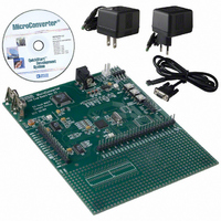
Evaluation Board, Power Supply, Cable, Software and Documentation
Silicon Manufacturer
Analog Devices
Core Architecture
8051
Silicon Core Number
ADuC831
Tool / Board Applications
General Purpose MCU, MPU, DSP, DSC
Mcu Supported Families
ADUC8xx
Development Tool Type
Hardware - Eval/Demo Board
Rohs Compliant
Yes
Lead Free Status / RoHS Status
Lead free / RoHS Compliant
For Use With/related Products
ADuC831
Lead Free Status / Rohs Status
Compliant
Other names
EVAL-ADUC831QS
EVAL-ADUC831QS
EVAL-ADUC831QS


Grounding and Board Layout Recommendations
As with all high resolution data converters, special attention must
be paid to grounding and PC board layout of ADuC831-based
designs in order to achieve optimum performance from the
ADC and DACs.
Although the ADuC831 has separate pins for analog and digital
ground (AGND and DGND), the user must not tie these to two
separate ground planes unless the two ground planes are con-
nected together very close to the ADuC831, as illustrated in the
simplified example of Figure 63a. In systems where digital and
analog ground planes are connected together somewhere else
(at the system’s power supply for example), they cannot be con-
nected again near the ADuC831 since a ground loop would result.
In these cases, tie the ADuC831’s AGND and DGND pins all
to the analog ground plane, as illustrated in Figure 63b. In systems
with only one ground plane, ensure that the digital and analog
components are physically separated onto separate halves of the
board such that digital return currents do not flow near analog
circuitry and vice versa. The ADuC831 can then be placed between
the digital and analog sections, as illustrated in Figure 63c.
In all of these scenarios, and in more complicated real-life applica-
tions, keep in mind the flow of current from the supplies and back
to ground. Make sure the return paths for all currents are as
close as possible to the paths the currents took to reach their desti-
nations. For example, do not power components on the analog
side of Figure 63b with DV
from DV
currents flowing under analog circuitry, which could happen if
the user placed a noisy digital chip on the left half of the board in
Figure 63c. Whenever possible, avoid large discontinuities in the
ground plane(s) (such as are formed by a long trace on the same
layer), since they force return signals to travel a longer path. And
of course, make all connections to the ground plane directly,
with little or no trace separating the pin from its via to ground.
Note that the bottom paddle of the CSP package should not
be connected to ground. It should be left unconnected.
If the user plans to connect fast logic signals (rise/fall time < 5 ns) to
any of the ADuC831’s digital inputs, add a series resistor to each
relevant line to keep rise and fall times longer than 5 ns at the
ADuC831 input pins. A value of 100 Ω or 200 Ω is usually suffi-
cient to prevent high speed signals from coupling capacitively into
the ADuC831 and affecting the accuracy of ADC conversions.
*Application Note uC006 is available at
REV. 0
DV
CORE RESET
INTERNAL
DD
2.45V TYP
1.0V TYP
DD
to flow through AGND. Also, try to avoid digital
Figure 62. Internal POR Operation
128ms TYP
DD
since that would force return currents
www.analog.com/microconverter
128ms TYP
1.0V TYP
–63–
OTHER HARDWARE CONSIDERATIONS
To facilitate in-circuit programming, plus in-circuit debug and
emulation options, users will want to implement some simple
connection points in their hardware that will allow easy access
to download, debug, and emulation modes.
In-Circuit Serial Download Access
Nearly all ADuC831 designs will want to take advantage of the
in-circuit reprogrammability of the chip. This is accomplished by
a connection to the ADuC831’s UART, which requires an exter-
nal RS-232 chip for level translation if downloading code from
a PC. Basic configuration of an RS-232 connection is illustrated
in Figure 66 with a simple ADM202-based circuit. If users would
rather not design an RS-232 chip onto a board, refer to the
application note “uC006–A 4-Wire UART-to-PC Interface”* for
a simple (and zero-cost-per-board) method of gaining in-circuit
serial download access to the ADuC831.
In addition to the basic UART connections, users will also need
a way to trigger the chip into download mode. This is accom-
plished via a 1 kΩ pull-down resistor that can be jumpered onto
the PSEN pin, as shown in Figure 64. To get the ADuC831 into
download mode, simply connect this jumper and power-cycle the
device (or manually reset the device, if a manual reset button is
available) and it will be ready to receive a new program serially.
With the jumper removed, the device will come up in normal
mode (and run the program) whenever power is cycled or RESET
is toggled.
a.
b.
c.
Figure 63. System Grounding Schemes
PLACE ANALOG
COMPONENTS
PLACE ANALOG
COMPONENTS
HERE
PLACE ANALOG
AGND
AGND
COMPONENTS
HERE
HERE
GND
PLACE DIGITAL
COMPONENTS
PLACE DIGITAL
COMPONENTS
PLACE DIGITAL
COMPONENTS
HERE
HERE
ADuC831
HERE
DGND
DGND
Related parts for EVAL-ADUC831QSZ
Image
Part Number
Description
Manufacturer
Datasheet
Request
R


Part Number:
Description:
BOARD EVAL FOR SI270X-A
Manufacturer:
Silicon Laboratories Inc
Datasheet:

Part Number:
Description:
BUCK CONV REF DESIGN KIT IP1201
Manufacturer:
International Rectifier
Datasheet:
Part Number:
Description:
BOARD DEMO SYNC DUAL BUCK CNVTER
Manufacturer:
International Rectifier
Datasheet:
Part Number:
Description:
BOARD DEMO SYNC BUCK CONVETER
Manufacturer:
International Rectifier
Datasheet:

Part Number:
Description:
EVALBOARD/EB Omnidirectional microphone - Analog
Manufacturer:
Analog Devices
Datasheet:
Part Number:
Description:
EVALBOARD/EB Omnidirectional microphone - Analog
Manufacturer:
Analog Devices
Datasheet:


Part Number:
Description:
BOARD EVAL LED DRIVER LT3756
Manufacturer:
Linear Technology
Datasheet:

Part Number:
Description:
BOARD EVAL FOR AD7741/7742
Manufacturer:
Analog Devices Inc
Datasheet:

Part Number:
Description:
±1.7g Dual-Axis IMEMS Accelerometer Evaluation Board
Manufacturer:
Analog Devices Inc
Datasheet:

Part Number:
Description:
IC MULTIPLIER ANALOG 8-SOIC T/R
Manufacturer:
Analog Devices Inc
Datasheet:

Part Number:
Description:
IC ANALOG MULTIPLIER 8-DIP
Manufacturer:
Analog Devices Inc
Datasheet:
Part Number:
Description:
IC ANALOG MULTIPLIER 8-SOIC
Manufacturer:
Analog Devices Inc
Datasheet:
Part Number:
Description:
IC ANALOG MULTIPLIER 8-DIP
Manufacturer:
Analog Devices Inc
Datasheet: