EVAL-ADUC831QSZ Analog Devices Inc, EVAL-ADUC831QSZ Datasheet - Page 6
EVAL-ADUC831QSZ
Manufacturer Part Number
EVAL-ADUC831QSZ
Description
KIT DEV FOR ADUC831 QUICK START
Manufacturer
Analog Devices Inc
Series
QuickStart™ Kitr
Type
MCUr
Datasheet
1.EVAL-ADUC831QSZ.pdf
(76 pages)
Specifications of EVAL-ADUC831QSZ
Contents
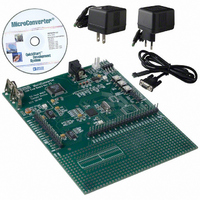
Evaluation Board, Power Supply, Cable, Software and Documentation
Silicon Manufacturer
Analog Devices
Core Architecture
8051
Silicon Core Number
ADuC831
Tool / Board Applications
General Purpose MCU, MPU, DSP, DSC
Mcu Supported Families
ADUC8xx
Development Tool Type
Hardware - Eval/Demo Board
Rohs Compliant
Yes
Lead Free Status / RoHS Status
Lead free / RoHS Compliant
For Use With/related Products
ADuC831
Lead Free Status / Rohs Status
Compliant
Other names
EVAL-ADUC831QS
EVAL-ADUC831QS
EVAL-ADUC831QS


SPECIFICATIONS
ADuC831
Parameter
POWER REQUIREMENTS
NOTES
10
11
12
13
14
15
16
17
18
19
20
Specifications subject to change without notice.
1
2
3
4
5
6
7
8
9
in unbuffered mode tested with OP270 external buffer, which has a low input leakage current.
decoupling capacitor chosen for both the V
pins need to be shorted together for correct operation.
25ºC is 700,000 cycles.
will derate with junction temperature as shown in Figure 18 in the Flash/EE Memory description section of this data sheet.
Temperature Range –40ºC to +125ºC.
ADC linearity is guaranteed during normal Micro Converter core operation.
ADC LSB Size = V
These numbers are not production tested but are guaranteed by design and/or characterization data on production release.
Offset and Gain Error and Offset and Gain Error Match are measured after factory calibration.
Based on external ADC system components, the user may need to execute a system calibration to remove additional external channel errors and achieve
these specifications.
SNR calculation includes distortion and noise components.
Channel-to-channel Crosstalk is measured on adjacent channels.
The Temperature Monitor will give a measure of the die temperature directly; air temperature can be inferred from this result.
DAC linearity is calculated using:
DAC differential nonlinearity specified on 0 to V
DAC specification for output impedance in the unbuffered case depends on DAC code.
DAC specifications for I
Measured with V
When using an external reference device, the internal band gap reference input can be bypassed by setting the ADCCON1.6 bit. In this mode the V
Flash/EE Memory reliability characteristics apply to both the Flash/EE program memory and the Flash/EE data memory.
Endurance is qualified to 100,000 cycles as per JEDEC Std. 22 method A117 and measured at -40ºC, +25ºC, and +125ºC. Typical endurance at
Retention lifetime equivalent at junction temperature (Tj) = 55ºC as per JEDEC Std. 22 method A117. Retention lifetime based on an activation energy of 0.6 eV
Power supply current consumption is measured in Normal, Idle, and Power-Down Modes under the following conditions:
DV
Power Supply Voltages
Power Supply Currents Normal Mode
Power Supply Currents Idle Mode
Power Supply Currents Power Down Mode
Typical Additional Power Supply Currents
DD
AV
DV
AV
DV
AV
DV
AV
DV
AV
AV
DV
PSM Peripheral
ADC
DAC
Reduced code range of 100 to 4095, 0 to V
Reduced code range of 100 to 3945, 0 to V
DAC Output Load = 10 kΩ and 100 pF.
Normal Mode:
Idle Mode:
Power-Down Mode: Reset = 0.4 V, All Port 0 pins = 0.4 V, All other digital I/O pins and Port 1 are open circuit, OSC off, TIC off.
power supply current will increase typically by 3 mA (3 V operation) and 10 mA (5 V operation) during a Flash/EE memory program or erase cycle.
DD
DD
DD
DD
DD
DD
DD
DD
DD
DD
DD
/DV
Current
Current
Current
Current
Current
Current
Current
Current
Current
Current
DD
REF
REF
to AGND
and C
4
/2
SINK
12
Reset = 0.4 V, Digital I/O pins = open circuit, Core Executing internal software loop.
Reset = 0.4 V, Digital I/O pins = open circuit, Core Execution suspended in idle mode.
i.e., for Internal V
REF
, voltage output settling time, and digital-to-analog glitch energy depend on external buffer implementation in unbuffered mode. DAC
pins decoupled with 0.1 µF capacitors to ground. Power-up time for the internal reference will be determined by the value of the
(continued)
19, 20
REF
REF
and C
REF
DD
= 2.5 V, 1 LSB = 610 V and for External V
REF
range.
range.
REF
and 0 to V
V
4.5
5.5
6
1.7
25
21
1.7
5
0.14
11
10
0.14
3
35
25
160
50
1.5
150
pins.
DD
= 5 V
DD
ranges
V
2.7
3.3
3
1.7
12
10
1.7
1
0.14
5
4
0.14
2.5
20
12
125
DD
–6–
= 3 V
REF
=1 V, 1 LSB = 244 V.
Unit
V min
V max
V min
V max
mA typ
mA max
mA max
mA typ
mA max
mA typ
mA typ
mA max
mA typ
mA typ
mA typ
A typ
A max
A typ
A typ
A typ
A typ
Test Conditions/Comments
AV
AV
MCLKIN = 1 MHz
MCLKIN = 1 MHz
MCLKIN = 16 MHz
MCLKIN = 16 MHz
MCLKIN = 16 MHz
MCLKIN = 1 MHz
MCLKIN = 1 MHz
MCLKIN = 16 MHz
MCLKIN = 16 MHz
MCLKIN = 16 MHz
MCLKIN = 2 MHz or 16 MHz
TIMECON.1 = 0
TIMECON.1 = 1
AV
DD
DD
DD
= DV
/DV
/DV
DD
DD
DD
= 3 V nom
= 5 V nom
= 5 V
REF
and C
REV. 0
REF
Related parts for EVAL-ADUC831QSZ
Image
Part Number
Description
Manufacturer
Datasheet
Request
R


Part Number:
Description:
BOARD EVAL FOR SI270X-A
Manufacturer:
Silicon Laboratories Inc
Datasheet:

Part Number:
Description:
BUCK CONV REF DESIGN KIT IP1201
Manufacturer:
International Rectifier
Datasheet:
Part Number:
Description:
BOARD DEMO SYNC DUAL BUCK CNVTER
Manufacturer:
International Rectifier
Datasheet:
Part Number:
Description:
BOARD DEMO SYNC BUCK CONVETER
Manufacturer:
International Rectifier
Datasheet:

Part Number:
Description:
EVALBOARD/EB Omnidirectional microphone - Analog
Manufacturer:
Analog Devices
Datasheet:
Part Number:
Description:
EVALBOARD/EB Omnidirectional microphone - Analog
Manufacturer:
Analog Devices
Datasheet:


Part Number:
Description:
BOARD EVAL LED DRIVER LT3756
Manufacturer:
Linear Technology
Datasheet:

Part Number:
Description:
BOARD EVAL FOR AD7741/7742
Manufacturer:
Analog Devices Inc
Datasheet:

Part Number:
Description:
±1.7g Dual-Axis IMEMS Accelerometer Evaluation Board
Manufacturer:
Analog Devices Inc
Datasheet:

Part Number:
Description:
IC MULTIPLIER ANALOG 8-SOIC T/R
Manufacturer:
Analog Devices Inc
Datasheet:

Part Number:
Description:
IC ANALOG MULTIPLIER 8-DIP
Manufacturer:
Analog Devices Inc
Datasheet:
Part Number:
Description:
IC ANALOG MULTIPLIER 8-SOIC
Manufacturer:
Analog Devices Inc
Datasheet:
Part Number:
Description:
IC ANALOG MULTIPLIER 8-DIP
Manufacturer:
Analog Devices Inc
Datasheet: