EVAL-ADUC831QSZ Analog Devices Inc, EVAL-ADUC831QSZ Datasheet - Page 39
EVAL-ADUC831QSZ
Manufacturer Part Number
EVAL-ADUC831QSZ
Description
KIT DEV FOR ADUC831 QUICK START
Manufacturer
Analog Devices Inc
Series
QuickStart™ Kitr
Type
MCUr
Datasheet
1.EVAL-ADUC831QSZ.pdf
(76 pages)
Specifications of EVAL-ADUC831QSZ
Contents
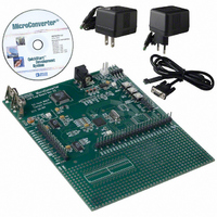
Evaluation Board, Power Supply, Cable, Software and Documentation
Silicon Manufacturer
Analog Devices
Core Architecture
8051
Silicon Core Number
ADuC831
Tool / Board Applications
General Purpose MCU, MPU, DSP, DSC
Mcu Supported Families
ADUC8xx
Development Tool Type
Hardware - Eval/Demo Board
Rohs Compliant
Yes
Lead Free Status / RoHS Status
Lead free / RoHS Compliant
For Use With/related Products
ADuC831
Lead Free Status / Rohs Status
Compliant
Other names
EVAL-ADUC831QS
EVAL-ADUC831QS
EVAL-ADUC831QS


SPIDAT
Function
SFR Address
Power-On Default Value
Bit Addressable
Using the SPI Interface
Depending on the configuration of the bits in the SPICON SFR
shown in Table XI, the ADuC831 SPI interface will transmit or
receive data in a number of possible modes. Figure 33 shows all
possible ADuC831 SPI configurations and the timing relation-
ships and synchronization between the signals involved. Also
shown in this figure is the SPI interrupt bit (ISPI) and how it is
triggered at the end of each byte-wide communication.
REV. 0
(CPHA = 0)
(CPHA = 1)
SAMPLE INPUT
DATA OUTPUT
SAMPLE INPUT
DATA OUTPUT
Figure 33. SPI Timing, All Modes
(CPOL = 1)
(CPOL = 0)
ISPI FLAG
ISPI FLAG
SCLOCK
SCLOCK
SS
?
MSB BIT 6 BIT 5
SPI Data Register
The SPIDAT SFR is written by the user to transmit data over the SPI interface or read by user code to
read data just received by the SPI interface.
F7H
00H
No
MSB BIT 6 BIT 5 BIT 4 BIT 3 BIT 2 BIT 1 LSB
BIT 4 BIT 3 BIT 2 BIT 1 LSB
?
–39–
SPI Interface—Master Mode
In master mode, the SCLOCK pin is always an output and gener-
ates a burst of eight clocks whenever user code writes to the
SPIDAT register. The SCLOCK bit rate is determined by
SPR0 and SPR1 in SPICON. It should also be noted that the
SS pin is not used in master mode. If the ADuC831 needs to
assert the SS pin on an external slave device, a port digital output
pin should be used.
In master mode, a byte transmission or reception is initiated
by a write to SPIDAT. Eight clock periods are generated via the
SCLOCK pin and the SPIDAT byte being transmitted via MOSI.
With each SCLOCK period a data bit is also sampled via MISO.
After eight clocks, the transmitted byte will have been completely
transmitted and the input byte will be waiting in the input shift
register. The ISPI flag will be set automatically and an interrupt
will occur if enabled. The value in the shift register will be latched
into SPIDAT.
SPI Interface—Slave Mode
In slave mode the SCLOCK is an input. The SS pin must
also be driven low externally during the byte communication.
Transmission is also initiated by a write to SPIDAT. In slave
mode, a data bit is transmitted via MISO and a data bit is received
via MOSI through each input SCLOCK period. After eight clocks,
the transmitted byte will have been completely transmitted and the
input byte will be waiting in the input shift register. The ISPI flag
will be set automatically and an interrupt will occur if enabled.
The value in the shift register will be latched into SPIDAT only
when the transmission/reception of a byte has been completed.
The end of transmission occurs after the eighth clock has been
received if CPHA = 1, or when SS returns high if CPHA = 0.
ADuC831
Related parts for EVAL-ADUC831QSZ
Image
Part Number
Description
Manufacturer
Datasheet
Request
R


Part Number:
Description:
BOARD EVAL FOR SI270X-A
Manufacturer:
Silicon Laboratories Inc
Datasheet:

Part Number:
Description:
BUCK CONV REF DESIGN KIT IP1201
Manufacturer:
International Rectifier
Datasheet:
Part Number:
Description:
BOARD DEMO SYNC DUAL BUCK CNVTER
Manufacturer:
International Rectifier
Datasheet:
Part Number:
Description:
BOARD DEMO SYNC BUCK CONVETER
Manufacturer:
International Rectifier
Datasheet:

Part Number:
Description:
EVALBOARD/EB Omnidirectional microphone - Analog
Manufacturer:
Analog Devices
Datasheet:
Part Number:
Description:
EVALBOARD/EB Omnidirectional microphone - Analog
Manufacturer:
Analog Devices
Datasheet:


Part Number:
Description:
BOARD EVAL LED DRIVER LT3756
Manufacturer:
Linear Technology
Datasheet:

Part Number:
Description:
BOARD EVAL FOR AD7741/7742
Manufacturer:
Analog Devices Inc
Datasheet:

Part Number:
Description:
±1.7g Dual-Axis IMEMS Accelerometer Evaluation Board
Manufacturer:
Analog Devices Inc
Datasheet:

Part Number:
Description:
IC MULTIPLIER ANALOG 8-SOIC T/R
Manufacturer:
Analog Devices Inc
Datasheet:

Part Number:
Description:
IC ANALOG MULTIPLIER 8-DIP
Manufacturer:
Analog Devices Inc
Datasheet:
Part Number:
Description:
IC ANALOG MULTIPLIER 8-SOIC
Manufacturer:
Analog Devices Inc
Datasheet:
Part Number:
Description:
IC ANALOG MULTIPLIER 8-DIP
Manufacturer:
Analog Devices Inc
Datasheet: