EVAL-ADUC831QSZ Analog Devices Inc, EVAL-ADUC831QSZ Datasheet - Page 24
EVAL-ADUC831QSZ
Manufacturer Part Number
EVAL-ADUC831QSZ
Description
KIT DEV FOR ADUC831 QUICK START
Manufacturer
Analog Devices Inc
Series
QuickStart™ Kitr
Type
MCUr
Datasheet
1.EVAL-ADUC831QSZ.pdf
(76 pages)
Specifications of EVAL-ADUC831QSZ
Contents
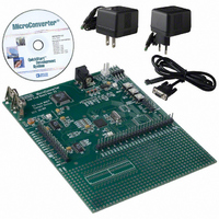
Evaluation Board, Power Supply, Cable, Software and Documentation
Silicon Manufacturer
Analog Devices
Core Architecture
8051
Silicon Core Number
ADuC831
Tool / Board Applications
General Purpose MCU, MPU, DSP, DSC
Mcu Supported Families
ADUC8xx
Development Tool Type
Hardware - Eval/Demo Board
Rohs Compliant
Yes
Lead Free Status / RoHS Status
Lead free / RoHS Compliant
For Use With/related Products
ADuC831
Lead Free Status / Rohs Status
Compliant
Other names
EVAL-ADUC831QS
EVAL-ADUC831QS
EVAL-ADUC831QS


ADuC831
Configuring the ADC
The ADuC831’s successive approximation ADC is driven by a
divided down version of the master clock. To ensure adequate
ADC operation, this ADC clock must be between 400 kHz and
6 MHz, and optimum performance is obtained with ADC clock
between 400 kHz and 4.5 MHz. Frequencies within this range
can easily be achieved with master clock frequencies from
400 kHz to well above 16 MHz with the four ADC clock divide
ratios to choose from. For example, with a 12 MHz master
clock, set the ADC clock divide ratio to 4 (i.e., ADCCLK =
MCLK/4 = 3 MHz) by setting the appropriate bits in
ADCCON1 (ADCCON1.5 = 1, ADCCON1.4 = 0).
The total ADC conversion time is 15 ADC clocks, plus 1 ADC
clock for synchronization, plus the selected acquisition time
(1, 2, 3, or 4 ADC clocks). For the example above, with three
clocks acquisition time, total conversion time is 19 ADC clocks
(or 6.3 µs for a 3 MHz ADC clock).
In continuous conversion mode, a new conversion begins each
time the previous one finishes. The sample rate is then simply
the inverse of the total conversion time described above. In the
example above, the continuous conversion mode sample rate
would be 157.8 kHz.
If using the temperature sensor as the ADC input, the ADC
should be configured to use an ADCCLK of MCLK/16 and
four acquisition clocks.
Increasing the conversion time on the temperature monitor
channel improves the accuracy of the reading. To further
improve the accuracy, an external reference with low tempera-
ture drift should also be used.
ADC DMA Mode
The on-chip ADC has been designed to run at a maximum
conversion speed of 4 µs (247 kHz sampling rate). When con-
verting at this rate, the ADuC831 MicroConverter has 4 µs to
read the ADC result and store the result in memory for further
postprocessing, otherwise the next ADC sample could be lost.
In an interrupt driven routine the MicroConverter would also
have to jump to the ADC Interrupt Service routine, which will
also increase the time required to store the ADC results. In
applications where the ADuC831 cannot sustain the interrupt
rate, an ADC DMA mode is provided.
To enable DMA mode, Bit 6 in ADCCON2 (DMA) must be
set. This allows the ADC results to be written directly to a
16 MByte external static memory SRAM (mapped into data
memory space) without any interaction from the ADuC831
core. This mode allows the ADuC831 to capture a contiguous
sample stream at full ADC update rates (247 kHz).
A Typical DMA Mode Configuration Example
To set the ADuC831 into DMA mode a number of steps must
be followed:
1. The ADC must be powered down. This is done by ensuring
2. The DMA address pointer must be set to the start address of
MD1 and MD0 are both set to 0 in ADCCON1.
where the ADC results are to be written. This is done by
writing to the DMA mode address pointers DMAL, DMAH,
and DMAP. DMAL must be written to first, followed by
DMAH, and then by DMAP.
–24–
3. The external memory must be preconfigured. This consists
4. The DMA is initiated by writing to the ADC SFRs in the
When the DMA conversions are completed, the ADC interrupt
bit ADCI, is set by hardware and the external SRAM contains
the new ADC conversion results as shown below. It should be
noted that no result is written to the last two memory locations.
When the DMA mode logic is active, it takes the responsibility of
storing the ADC results away from both the user and ADuC831
core logic. As it writes the results of the ADC conversions to
external memory, it takes over the external memory interface
from the core. Thus, any core instructions that access the external
memory while DMA mode is enabled will not get access to it. The
core will execute the instructions and they will take the same time
to execute but they will not gain access to the external memory.
Figure 14. Typical DMA External Memory Preconfiguration
00000AH
000000H
00000AH
000000H
of writing the required ADC channel IDs into the top four
bits of every second memory location in the external SRAM
starting at the first address specified by the DMA address
pointer. As the ADC DMA mode operates independent from
the ADuC831 core, it is necessary to provide it with a stop
command. This is done by duplicating the last channel ID to
be converted followed by “1111” into the next channel selec-
tion field. A typical preconfiguration of external memory is
as follows.
following sequence:
a. ADCCON2 is written to enable the DMA mode, i.e.,
b. ADCCON1 is written to configure the conversion time and
c. ADC conversions are initiated. This is done by starting
Figure 15. Typical External Memory Configuration
Post ADC DMA Operation
MOV ADCCON2, #40H; DMA mode enabled.
power-up of the ADC. It can also enable Timer 2 driven
conversions or external triggered conversions if required.
single conversions, starting Timer 2 running for Timer 2
conversions or by receiving an external trigger.
1
0
0
1
0
0
1
0
0
1
0
0
1
0
0
0
1
0
1
0
0
0
1
0
0
0
0
0
1
1
1
1
1
1
1
1
1
1
1
0
1
0
1
1
1
0
1
0
STOP COMMAND
REPEAT LAST CHANNEL
FOR A VALID STOP
CONDITION
CONVERT ADC CH#3
CONVERT TEMP SENSOR
CONVERT ADC CH#5
CONVERT ADC CH#2
STOP COMMAND
NO CONVERSION
RESULT WRITTEN HERE
CONVERSION RESULT
FOR ADC CH#3
CONVERSION RESULT
FOR TEMP SENSOR
CONVERSION RESULT
FOR ADC CH#5
CONVERSION RESULT
FOR ADC CH#2
REV. 0
Related parts for EVAL-ADUC831QSZ
Image
Part Number
Description
Manufacturer
Datasheet
Request
R


Part Number:
Description:
BOARD EVAL FOR SI270X-A
Manufacturer:
Silicon Laboratories Inc
Datasheet:

Part Number:
Description:
BUCK CONV REF DESIGN KIT IP1201
Manufacturer:
International Rectifier
Datasheet:
Part Number:
Description:
BOARD DEMO SYNC DUAL BUCK CNVTER
Manufacturer:
International Rectifier
Datasheet:
Part Number:
Description:
BOARD DEMO SYNC BUCK CONVETER
Manufacturer:
International Rectifier
Datasheet:

Part Number:
Description:
EVALBOARD/EB Omnidirectional microphone - Analog
Manufacturer:
Analog Devices
Datasheet:
Part Number:
Description:
EVALBOARD/EB Omnidirectional microphone - Analog
Manufacturer:
Analog Devices
Datasheet:


Part Number:
Description:
BOARD EVAL LED DRIVER LT3756
Manufacturer:
Linear Technology
Datasheet:

Part Number:
Description:
BOARD EVAL FOR AD7741/7742
Manufacturer:
Analog Devices Inc
Datasheet:

Part Number:
Description:
±1.7g Dual-Axis IMEMS Accelerometer Evaluation Board
Manufacturer:
Analog Devices Inc
Datasheet:

Part Number:
Description:
IC MULTIPLIER ANALOG 8-SOIC T/R
Manufacturer:
Analog Devices Inc
Datasheet:

Part Number:
Description:
IC ANALOG MULTIPLIER 8-DIP
Manufacturer:
Analog Devices Inc
Datasheet:
Part Number:
Description:
IC ANALOG MULTIPLIER 8-SOIC
Manufacturer:
Analog Devices Inc
Datasheet:
Part Number:
Description:
IC ANALOG MULTIPLIER 8-DIP
Manufacturer:
Analog Devices Inc
Datasheet: