EVAL-ADUC831QSZ Analog Devices Inc, EVAL-ADUC831QSZ Datasheet - Page 35
EVAL-ADUC831QSZ
Manufacturer Part Number
EVAL-ADUC831QSZ
Description
KIT DEV FOR ADUC831 QUICK START
Manufacturer
Analog Devices Inc
Series
QuickStart™ Kitr
Type
MCUr
Datasheet
1.EVAL-ADUC831QSZ.pdf
(76 pages)
Specifications of EVAL-ADUC831QSZ
Contents
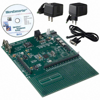
Evaluation Board, Power Supply, Cable, Software and Documentation
Silicon Manufacturer
Analog Devices
Core Architecture
8051
Silicon Core Number
ADuC831
Tool / Board Applications
General Purpose MCU, MPU, DSP, DSC
Mcu Supported Families
ADUC8xx
Development Tool Type
Hardware - Eval/Demo Board
Rohs Compliant
Yes
Lead Free Status / RoHS Status
Lead free / RoHS Compliant
For Use With/related Products
ADuC831
Lead Free Status / Rohs Status
Compliant
Other names
EVAL-ADUC831QS
EVAL-ADUC831QS
EVAL-ADUC831QS


PULSEWIDTH MODULATOR (PWM)
The PWM on the ADuC831 is highly flexible PWM offering
programmable resolution and input clock, and can be config-
ured for any one of six different modes of operation. Two of
these modes allow the PWM to be configured as a - DAC
with up to 16 bits of resolution. A block diagram of the PWM is
shown in Figure 26.
Bit
7
6
5
4
3
2
1
0
REV. 0
T0/ EXTERNAL PWM CLOCK
f
OSC
f
OSC
/DIVIDE FACTOR/15
Name
SNGL
MD2
MD1
MD0
CDIV1
CDIV0
CSEL1
CSEL0
/DIVIDE FACTOR
Figure 26. PWM Block Diagram
f
OSC
SELECT
CLOCK
Description
Turns Off PWM output at P2.6 or P3.4 Leaving Port Pin Free for Digital I/O.
PWM Mode Bits
The MD2/1/0 bits choose the PWM mode as follows:
MD2
0
0
0
0
1
1
1
1
PWM Clock Divider
Scale the clock source for the PWM counter as shown below:
CDIV1 CDIV0 Description
0
0
1
1
PWM Clock Divider
Select the clock source for the PWM as shown below:
CSEL1 CSEL0 Description
0
0
1
1
MODE
16-BIT PWM COUNTER
MD1
0
0
1
1
0
0
1
1
0
1
0
1
0
1
0
1
PROGRAMMABLE
COMPARE
PWM0H/L
DIVIDER
Table X. PWMCON SFR Bit Designations
MD0
0
1
0
1
0
1
0
1
PWM Counter = Selected Clock/1
PWM Counter = Selected Clock/4
PWM Counter = Selected Clock/16
PWM Counter = Selected Clock/64
PWM Clock = f
PWM Clock = f
PWM Clock = External input at P3.4/T0
PWM Clock = f
PWM1H/L
Mode
Mode 0: PWM Disabled
Mode 1: Single variable resolution PWM on P2.7 or P3.3
Mode 2: Twin 8-bit PWM
Mode 3: Twin 16-bit PWM
Mode 4: Dual NRZ 16-bit Σ-∆ DAC
Mode 5: Dual 8-bit PWM
Mode 6: Dual RZ 16-bit Σ-∆ DAC
Reserved for future use
P2.6
P2.7
OCS/DIVIDE FACTOR
OCS/DIVIDE FACTOR
OSC
–35–
The PWM uses five SFRs: the control SFR (PWMCON), and
four data SFRs (PWM0H, PWM0L, PWM1H, and PWM1L).
PWMCON (as described below) controls the different modes of
operation of the PWM as well as the PWM clock frequency.
PWM0H/L and PWM1H/L are the data registers that determine
the duty cycles of the PWM outputs. The output pins that the
PWM uses are determined by the CFG831 register and they can
be either P2.6 and P2.7 or P3.4 and P3.3. In this section of the
data sheet, it is assumed that P2.6 and P2.7 are selected as the
PWM outputs.
To use the PWM user software, first write to PWMCON to select
the PWM mode of operation and the PWM input clock. Writing
to PWMCON also resets the PWM counter. In any of the 16-bit
modes of operation (modes 1, 3, 4, 6), user software should
write to the PWM0L or PWM1L SFRs first. This value is written
to a hidden SFR. Writing to the PWM0H or PWM1H SFRs
updates both the PWMxH and the PWMxL SFRs but does not
change the outputs until the end of the PWM cycle in progress.
The values written to these 16-bit registers are then used in the
next PWM cycle.
PWMCON
SFR Address
Power-On Default Value
Bit Addressable
/15 (see CFG831 register)
(see CFG831 register)
PWM Control SFR
AEH
00H
No
ADuC831
Related parts for EVAL-ADUC831QSZ
Image
Part Number
Description
Manufacturer
Datasheet
Request
R


Part Number:
Description:
BOARD EVAL FOR SI270X-A
Manufacturer:
Silicon Laboratories Inc
Datasheet:

Part Number:
Description:
BUCK CONV REF DESIGN KIT IP1201
Manufacturer:
International Rectifier
Datasheet:
Part Number:
Description:
BOARD DEMO SYNC DUAL BUCK CNVTER
Manufacturer:
International Rectifier
Datasheet:
Part Number:
Description:
BOARD DEMO SYNC BUCK CONVETER
Manufacturer:
International Rectifier
Datasheet:

Part Number:
Description:
EVALBOARD/EB Omnidirectional microphone - Analog
Manufacturer:
Analog Devices
Datasheet:
Part Number:
Description:
EVALBOARD/EB Omnidirectional microphone - Analog
Manufacturer:
Analog Devices
Datasheet:


Part Number:
Description:
BOARD EVAL LED DRIVER LT3756
Manufacturer:
Linear Technology
Datasheet:

Part Number:
Description:
BOARD EVAL FOR AD7741/7742
Manufacturer:
Analog Devices Inc
Datasheet:

Part Number:
Description:
±1.7g Dual-Axis IMEMS Accelerometer Evaluation Board
Manufacturer:
Analog Devices Inc
Datasheet:

Part Number:
Description:
IC MULTIPLIER ANALOG 8-SOIC T/R
Manufacturer:
Analog Devices Inc
Datasheet:

Part Number:
Description:
IC ANALOG MULTIPLIER 8-DIP
Manufacturer:
Analog Devices Inc
Datasheet:
Part Number:
Description:
IC ANALOG MULTIPLIER 8-SOIC
Manufacturer:
Analog Devices Inc
Datasheet:
Part Number:
Description:
IC ANALOG MULTIPLIER 8-DIP
Manufacturer:
Analog Devices Inc
Datasheet: