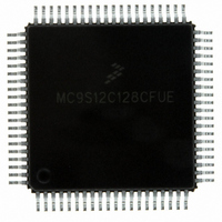
MC9S12C128CFUE Freescale Semiconductor, MC9S12C128CFUE Datasheet - Page 178

MC9S12C128CFUE
Manufacturer Part Number
MC9S12C128CFUE
Description
IC MCU 128K FLASH 25MHZ 80-QFP
Manufacturer
Freescale Semiconductor
Series
HCS12r
Specifications of MC9S12C128CFUE
Core Processor
HCS12
Core Size
16-Bit
Speed
25MHz
Connectivity
CAN, EBI/EMI, SCI, SPI
Peripherals
POR, PWM, WDT
Number Of I /o
60
Program Memory Size
128KB (128K x 8)
Program Memory Type
FLASH
Ram Size
4K x 8
Voltage - Supply (vcc/vdd)
2.35 V ~ 5.5 V
Data Converters
A/D 8x10b
Oscillator Type
Internal
Operating Temperature
-40°C ~ 85°C
Package / Case
80-QFP
Cpu Family
HCS12
Device Core Size
16b
Frequency (max)
25MHz
Interface Type
CAN/SCI/SPI
Total Internal Ram Size
4KB
# I/os (max)
60
Number Of Timers - General Purpose
8
Operating Supply Voltage (typ)
2.5/5V
Operating Supply Voltage (max)
2.75/5.5V
Operating Supply Voltage (min)
2.35/2.97V
On-chip Adc
8-chx10-bit
Instruction Set Architecture
CISC
Operating Temp Range
-40C to 85C
Operating Temperature Classification
Industrial
Mounting
Surface Mount
Pin Count
80
Package Type
PQFP
Processor Series
S12C
Core
HCS12
Data Bus Width
16 bit
Data Ram Size
4000 B
Maximum Clock Frequency
25 MHz
Number Of Programmable I/os
61
Number Of Timers
1
Operating Supply Voltage
- 0.3 V to + 6.5 V
Maximum Operating Temperature
+ 85 C
Mounting Style
SMD/SMT
3rd Party Development Tools
EWHCS12
Development Tools By Supplier
M68EVB912C32EE
Minimum Operating Temperature
- 40 C
Lead Free Status / RoHS Status
Lead free / RoHS Compliant
Eeprom Size
-
Lead Free Status / Rohs Status
Compliant
Available stocks
Company
Part Number
Manufacturer
Quantity
Price
Company:
Part Number:
MC9S12C128CFUE
Manufacturer:
ST
Quantity:
6 246
Company:
Part Number:
MC9S12C128CFUE
Manufacturer:
Freescale Semiconductor
Quantity:
10 000
- Current page: 178 of 690
- Download datasheet (4Mb)
Chapter 6 Background Debug Module (BDMV4) Block Description
For hardware data read commands, the external host must wait 150 bus clock cycles after sending the
address before attempting to obtain the read data. This is to be certain that valid data is available in the
BDM shift register, ready to be shifted out. For hardware write commands, the external host must wait
150 bus clock cycles after sending the data to be written before attempting to send a new command. This
is to avoid disturbing the BDM shift register before the write has been completed. The 150 bus clock cycle
delay in both cases includes the maximum 128 cycle delay that can be incurred as the BDM waits for a
free cycle before stealing a cycle.
For firmware read commands, the external host should wait 44 bus clock cycles after sending the command
opcode and before attempting to obtain the read data. This includes the potential of an extra 7 cycles when
the access is external with a narrow bus access (+1 cycle) and / or a stretch (+1, 2, or 3 cycles), (7 cycles
could be needed if both occur). The 44 cycle wait allows enough time for the requested data to be made
available in the BDM shift register, ready to be shifted out.
For firmware write commands, the external host must wait 32 bus clock cycles after sending the data to be
written before attempting to send a new command. This is to avoid disturbing the BDM shift register
before the write has been completed.
The external host should wait 64 bus clock cycles after a TRACE1 or GO command before starting any
new serial command. This is to allow the CPU to exit gracefully from the standard BDM firmware lookup
table and resume execution of the user code. Disturbing the BDM shift register prematurely may adversely
affect the exit from the standard BDM firmware lookup table.
Figure 6-6
times starting with a falling edge. The bar across the top of the blocks indicates that the BKGD line idles
in the high state. The time for an 8-bit command is 8 × 16 target clock cycles.
1. Target clock cycles are cycles measured using the target MCU’s serial clock rate. See
and
178
Section 6.3.2.1, “BDM Status Register
represents the BDM command structure. The command blocks illustrate a series of eight bit
16-bit misaligned reads and writes are not allowed. If attempted, the BDM
will ignore the least significant bit of the address and will assume an even
address from the remaining bits.
This timing has increased from previous BDM modules due to the new
capability in which the BDM serial interface can potentially run faster than
the bus. On previous BDM modules this extra time could be hidden within
the serial time.
If the bus rate of the target processor is unknown or could be changing, it is
recommended that the ACK (acknowledge function) be used to indicate
when an operation is complete. When using ACK, the delay times are
automated.
(BDMSTS),” for information on how serial clock rate is selected.
MC9S12C-Family / MC9S12GC-Family
Rev 01.24
NOTE
NOTE
NOTE
Section 6.4.6, “BDM Serial
1
Freescale Semiconductor
Interface,”
Related parts for MC9S12C128CFUE
Image
Part Number
Description
Manufacturer
Datasheet
Request
R
Part Number:
Description:
Manufacturer:
Freescale Semiconductor, Inc
Datasheet:
Part Number:
Description:
Manufacturer:
Freescale Semiconductor, Inc
Datasheet:
Part Number:
Description:
Manufacturer:
Freescale Semiconductor, Inc
Datasheet:
Part Number:
Description:
Manufacturer:
Freescale Semiconductor, Inc
Datasheet:
Part Number:
Description:
Manufacturer:
Freescale Semiconductor, Inc
Datasheet:
Part Number:
Description:
Manufacturer:
Freescale Semiconductor, Inc
Datasheet:
Part Number:
Description:
Manufacturer:
Freescale Semiconductor, Inc
Datasheet:
Part Number:
Description:
Manufacturer:
Freescale Semiconductor, Inc
Datasheet:
Part Number:
Description:
Manufacturer:
Freescale Semiconductor, Inc
Datasheet:
Part Number:
Description:
Manufacturer:
Freescale Semiconductor, Inc
Datasheet:
Part Number:
Description:
Manufacturer:
Freescale Semiconductor, Inc
Datasheet:
Part Number:
Description:
Manufacturer:
Freescale Semiconductor, Inc
Datasheet:
Part Number:
Description:
Manufacturer:
Freescale Semiconductor, Inc
Datasheet:
Part Number:
Description:
Manufacturer:
Freescale Semiconductor, Inc
Datasheet:
Part Number:
Description:
Manufacturer:
Freescale Semiconductor, Inc
Datasheet:


