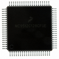
MC9S12C128CFUE Freescale Semiconductor, MC9S12C128CFUE Datasheet - Page 233

MC9S12C128CFUE
Manufacturer Part Number
MC9S12C128CFUE
Description
IC MCU 128K FLASH 25MHZ 80-QFP
Manufacturer
Freescale Semiconductor
Series
HCS12r
Specifications of MC9S12C128CFUE
Core Processor
HCS12
Core Size
16-Bit
Speed
25MHz
Connectivity
CAN, EBI/EMI, SCI, SPI
Peripherals
POR, PWM, WDT
Number Of I /o
60
Program Memory Size
128KB (128K x 8)
Program Memory Type
FLASH
Ram Size
4K x 8
Voltage - Supply (vcc/vdd)
2.35 V ~ 5.5 V
Data Converters
A/D 8x10b
Oscillator Type
Internal
Operating Temperature
-40°C ~ 85°C
Package / Case
80-QFP
Cpu Family
HCS12
Device Core Size
16b
Frequency (max)
25MHz
Interface Type
CAN/SCI/SPI
Total Internal Ram Size
4KB
# I/os (max)
60
Number Of Timers - General Purpose
8
Operating Supply Voltage (typ)
2.5/5V
Operating Supply Voltage (max)
2.75/5.5V
Operating Supply Voltage (min)
2.35/2.97V
On-chip Adc
8-chx10-bit
Instruction Set Architecture
CISC
Operating Temp Range
-40C to 85C
Operating Temperature Classification
Industrial
Mounting
Surface Mount
Pin Count
80
Package Type
PQFP
Processor Series
S12C
Core
HCS12
Data Bus Width
16 bit
Data Ram Size
4000 B
Maximum Clock Frequency
25 MHz
Number Of Programmable I/os
61
Number Of Timers
1
Operating Supply Voltage
- 0.3 V to + 6.5 V
Maximum Operating Temperature
+ 85 C
Mounting Style
SMD/SMT
3rd Party Development Tools
EWHCS12
Development Tools By Supplier
M68EVB912C32EE
Minimum Operating Temperature
- 40 C
Lead Free Status / RoHS Status
Lead free / RoHS Compliant
Eeprom Size
-
Lead Free Status / Rohs Status
Compliant
Available stocks
Company
Part Number
Manufacturer
Quantity
Price
Company:
Part Number:
MC9S12C128CFUE
Manufacturer:
ST
Quantity:
6 246
Company:
Part Number:
MC9S12C128CFUE
Manufacturer:
Freescale Semiconductor
Quantity:
10 000
- Current page: 233 of 690
- Download datasheet (4Mb)
Freescale Semiconductor
FRIZ[1:0]
Field
FIFO
1–0
2
Result Register FIFO Mode — If this bit is zero (non-FIFO mode), the A/D conversion results map into the result
registers based on the conversion sequence; the result of the first conversion appears in the first result register,
the second result in the second result register, and so on.
If this bit is one (FIFO mode) the conversion counter is not reset at the beginning or ending of a conversion
sequence; sequential conversion results are placed in consecutive result registers. In a continuously scanning
conversion sequence, the result register counter will wrap around when it reaches the end of the result register
file. The conversion counter value (CC2-0 in ATDSTAT0) can be used to determine where in the result register
file, the current conversion result will be placed.
Aborting a conversion or starting a new conversion by write to an ATDCTL register (ATDCTL5-0) clears the
conversion counter even if FIFO=1. So the first result of a new conversion sequence, started by writing to
ATDCTL5, will always be place in the first result register (ATDDDR0). Intended usage of FIFO mode is continuos
conversion (SCAN=1) or triggered conversion (ETRIG=1).
Which result registers hold valid data can be tracked using the conversion complete flags. Fast flag clear mode
may or may not be useful in a particular application to track valid data.
0 Conversion results are placed in the corresponding result register up to the selected sequence length.
1 Conversion results are placed in consecutive result registers (wrap around at end).
Background Debug Freeze Enable — When debugging an application, it is useful in many cases to have the
ATD pause when a breakpoint (Freeze Mode) is encountered. These 2 bits determine how the ATD will respond
to a breakpoint as shown in
compromise the accuracy of an immediately frozen conversion depending on the length of the freeze period.
S8C
0
0
0
0
0
0
0
0
1
FRZ1
0
0
1
1
Table 8-5. ATD Behavior in Freeze Mode (Breakpoint)
Table 8-3. ATDCTL3 Field Descriptions (continued)
Table 8-4. Conversion Sequence Length Coding
S4C
X
0
0
0
0
1
1
1
1
Table
MC9S12C-Family / MC9S12GC-Family
FRZ0
0
1
0
1
8-5. Leakage onto the storage node and comparator reference capacitors may
S2C
0
0
1
1
0
0
1
1
X
Rev 01.24
Finish current conversion, then freeze
Chapter 8 Analog-to-Digital Converter (ATD10B8C) Block Description
S1C
X
Description
0
1
0
1
0
1
0
1
Behavior in Freeze Mode
Continue conversion
Freeze Immediately
Number of Conversions per
Reserved
Sequence
8
1
2
3
4
5
6
7
8
233
Related parts for MC9S12C128CFUE
Image
Part Number
Description
Manufacturer
Datasheet
Request
R
Part Number:
Description:
Manufacturer:
Freescale Semiconductor, Inc
Datasheet:
Part Number:
Description:
Manufacturer:
Freescale Semiconductor, Inc
Datasheet:
Part Number:
Description:
Manufacturer:
Freescale Semiconductor, Inc
Datasheet:
Part Number:
Description:
Manufacturer:
Freescale Semiconductor, Inc
Datasheet:
Part Number:
Description:
Manufacturer:
Freescale Semiconductor, Inc
Datasheet:
Part Number:
Description:
Manufacturer:
Freescale Semiconductor, Inc
Datasheet:
Part Number:
Description:
Manufacturer:
Freescale Semiconductor, Inc
Datasheet:
Part Number:
Description:
Manufacturer:
Freescale Semiconductor, Inc
Datasheet:
Part Number:
Description:
Manufacturer:
Freescale Semiconductor, Inc
Datasheet:
Part Number:
Description:
Manufacturer:
Freescale Semiconductor, Inc
Datasheet:
Part Number:
Description:
Manufacturer:
Freescale Semiconductor, Inc
Datasheet:
Part Number:
Description:
Manufacturer:
Freescale Semiconductor, Inc
Datasheet:
Part Number:
Description:
Manufacturer:
Freescale Semiconductor, Inc
Datasheet:
Part Number:
Description:
Manufacturer:
Freescale Semiconductor, Inc
Datasheet:
Part Number:
Description:
Manufacturer:
Freescale Semiconductor, Inc
Datasheet:


