MC9S12C128CFUE Freescale Semiconductor, MC9S12C128CFUE Datasheet - Page 234
MC9S12C128CFUE
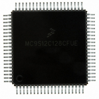
Manufacturer Part Number
MC9S12C128CFUE
Description
IC MCU 128K FLASH 25MHZ 80-QFP
Manufacturer
Freescale Semiconductor
Series
HCS12r
Specifications of MC9S12C128CFUE
Core Processor
HCS12
Core Size
16-Bit
Speed
25MHz
Connectivity
CAN, EBI/EMI, SCI, SPI
Peripherals
POR, PWM, WDT
Number Of I /o
60
Program Memory Size
128KB (128K x 8)
Program Memory Type
FLASH
Ram Size
4K x 8
Voltage - Supply (vcc/vdd)
2.35 V ~ 5.5 V
Data Converters
A/D 8x10b
Oscillator Type
Internal
Operating Temperature
-40°C ~ 85°C
Package / Case
80-QFP
Cpu Family
HCS12
Device Core Size
16b
Frequency (max)
25MHz
Interface Type
CAN/SCI/SPI
Total Internal Ram Size
4KB
# I/os (max)
60
Number Of Timers - General Purpose
8
Operating Supply Voltage (typ)
2.5/5V
Operating Supply Voltage (max)
2.75/5.5V
Operating Supply Voltage (min)
2.35/2.97V
On-chip Adc
8-chx10-bit
Instruction Set Architecture
CISC
Operating Temp Range
-40C to 85C
Operating Temperature Classification
Industrial
Mounting
Surface Mount
Pin Count
80
Package Type
PQFP
Processor Series
S12C
Core
HCS12
Data Bus Width
16 bit
Data Ram Size
4000 B
Maximum Clock Frequency
25 MHz
Number Of Programmable I/os
61
Number Of Timers
1
Operating Supply Voltage
- 0.3 V to + 6.5 V
Maximum Operating Temperature
+ 85 C
Mounting Style
SMD/SMT
3rd Party Development Tools
EWHCS12
Development Tools By Supplier
M68EVB912C32EE
Minimum Operating Temperature
- 40 C
Lead Free Status / RoHS Status
Lead free / RoHS Compliant
Eeprom Size
-
Lead Free Status / Rohs Status
Compliant
Available stocks
Company
Part Number
Manufacturer
Quantity
Price
Company:

Part Number:
MC9S12C128CFUE
Manufacturer:
ST
Quantity:
6 246
Company:
Part Number:
MC9S12C128CFUE
Manufacturer:
Freescale Semiconductor
Quantity:
10 000


Chapter 8 Analog-to-Digital Converter (ATD10B8C) Block Description
8.3.2.5
This register selects the conversion clock frequency, the length of the second phase of the sample time and
the resolution of the A/D conversion (i.e.: 8-bits or 10-bits). Writes to this register will abort current
conversion sequence but will not start a new sequence.
Read: Anytime
Write: Anytime
234
Module Base + 0x0004
SMP[1:0]
PRS[4:0}
SRES8
Reset
Field
6–5
4–0
7
W
R
SRES8
A/D Resolution Select — This bit selects the resolution of A/D conversion results as either 8 or 10 bits. The A/D
converter has an accuracy of 10 bits; however, if low resolution is required, the conversion can be speeded up
by selecting 8-bit resolution.
0 10-bit resolution
1 8-bit resolution
Sample Time Select — These two bits select the length of the second phase of the sample time in units of ATD
conversion clock cycles. Note that the ATD conversion clock period is itself a function of the prescaler value (bits
PRS4-0). The sample time consists of two phases. The first phase is two ATD conversion clock cycles long and
transfers the sample quickly (via the buffer amplifier) onto the A/D machine’s storage node. The second phase
attaches the external analog signal directly to the storage node for final charging and high accuracy.
lists the lengths available for the second sample phase.
ATD Clock Prescaler — These 5 bits are the binary value prescaler value PRS. The ATD conversion clock
frequency is calculated as follows:
Note: The maximum ATD conversion clock frequency is half the Bus Clock. The default (after reset) prescaler
ATD Control Register 4 (ATDCTL4)
0
7
value is 5 which results in a default ATD conversion clock frequency that is Bus Clock divided by 12.
Table 8-8
ATDclock
SMP1
0
0
1
1
SMP1
0
6
illustrates the divide-by operation and the appropriate range of the Bus Clock.
=
Figure 8-7. ATD Control Register 4 (ATDCTL4)
[
----------------------------- -
BusClock
[
PRS
Table 8-6. ATDCTL4 Field Descriptions
SMP0
SMP0
MC9S12C-Family / MC9S12GC-Family
+
0
1
0
1
Table 8-7. Sample Time Select
0
1
5
]
]
×
0.5
PRS4
Rev 01.24
0
4
Length of 2nd Phase of Sample Time
Description
16 A/D conversion clock periods
2 A/D conversion clock periods
4 A/D conversion clock periods
8 A/D conversion clock periods
PRS3
0
3
PRS2
1
2
Freescale Semiconductor
PRS1
0
1
Table 8-7
PRS0
1
0
Related parts for MC9S12C128CFUE
Image
Part Number
Description
Manufacturer
Datasheet
Request
R

Part Number:
Description:
Manufacturer:
Freescale Semiconductor, Inc
Datasheet:
Part Number:
Description:
Manufacturer:
Freescale Semiconductor, Inc
Datasheet:
Part Number:
Description:
Manufacturer:
Freescale Semiconductor, Inc
Datasheet:
Part Number:
Description:
Manufacturer:
Freescale Semiconductor, Inc
Datasheet:
Part Number:
Description:
Manufacturer:
Freescale Semiconductor, Inc
Datasheet:
Part Number:
Description:
Manufacturer:
Freescale Semiconductor, Inc
Datasheet:
Part Number:
Description:
Manufacturer:
Freescale Semiconductor, Inc
Datasheet:
Part Number:
Description:
Manufacturer:
Freescale Semiconductor, Inc
Datasheet:
Part Number:
Description:
Manufacturer:
Freescale Semiconductor, Inc
Datasheet:
Part Number:
Description:
Manufacturer:
Freescale Semiconductor, Inc
Datasheet:
Part Number:
Description:
Manufacturer:
Freescale Semiconductor, Inc
Datasheet:
Part Number:
Description:
Manufacturer:
Freescale Semiconductor, Inc
Datasheet:
Part Number:
Description:
Manufacturer:
Freescale Semiconductor, Inc
Datasheet:
Part Number:
Description:
Manufacturer:
Freescale Semiconductor, Inc
Datasheet:
Part Number:
Description:
Manufacturer:
Freescale Semiconductor, Inc
Datasheet: