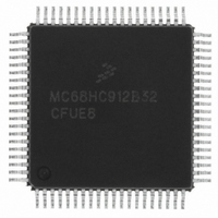
MCHC912B32CFUE8 Freescale Semiconductor, MCHC912B32CFUE8 Datasheet - Page 138

MCHC912B32CFUE8
Manufacturer Part Number
MCHC912B32CFUE8
Description
IC MCU 32K FLASH 8MHZ 80-QFP
Manufacturer
Freescale Semiconductor
Series
HC12r
Datasheet
1.MCHC912B32CFUE8.pdf
(334 pages)
Specifications of MCHC912B32CFUE8
Core Processor
CPU12
Core Size
16-Bit
Speed
8MHz
Connectivity
SCI, SPI
Peripherals
POR, PWM, WDT
Number Of I /o
63
Program Memory Size
32KB (32K x 8)
Program Memory Type
FLASH
Eeprom Size
768 x 8
Ram Size
1K x 8
Voltage - Supply (vcc/vdd)
4.5 V ~ 5.5 V
Data Converters
A/D 8x10b
Oscillator Type
External
Operating Temperature
-40°C ~ 85°C
Package / Case
80-QFP
Cpu Family
HC12
Device Core Size
16b
Frequency (max)
8MHz
Interface Type
SCI/SPI
Total Internal Ram Size
1KB
# I/os (max)
63
Operating Supply Voltage (typ)
5V
Operating Supply Voltage (max)
5.5V
Operating Supply Voltage (min)
4.5V
On-chip Adc
8-chx10-bit
Instruction Set Architecture
CISC
Operating Temp Range
-40C to 85C
Operating Temperature Classification
Industrial
Mounting
Surface Mount
Pin Count
80
Package Type
PQFP
Package
80PQFP
Family Name
HC12
Maximum Speed
8 MHz
Operating Supply Voltage
5 V
Data Bus Width
16 Bit
Number Of Programmable I/os
63
Processor Series
HC912B
Core
HC12
Data Ram Size
1 KB
Maximum Clock Frequency
8 MHz
Maximum Operating Temperature
+ 85 C
Mounting Style
SMD/SMT
3rd Party Development Tools
EWHCS12
Development Tools By Supplier
M68EVB912B32E
Minimum Operating Temperature
- 40 C
Lead Free Status / RoHS Status
Lead free / RoHS Compliant
Available stocks
Company
Part Number
Manufacturer
Quantity
Price
Company:
Part Number:
MCHC912B32CFUE8
Manufacturer:
Freescale Semiconductor
Quantity:
10 000
- Current page: 138 of 334
- Download datasheet (2Mb)
Pulse-Width Modulator (PWM)
11.2.15 Port P Data Direction Register
Read: Anytime
Write: Anytime
DDRP determines pin direction of port P when used for general-purpose I/O. When cleared, I/O pin is
configured for input. When set, I/O pin is configured for output.
11.3 PWM Boundary Cases
The boundary conditions for the PWM channel duty registers and the PWM channel period registers
cause the results shown in
11.4 Using the Output Compare 7 Feature to Generate a PWM
This timer exercise is intended to utilize the output compare function along with the output compare 7 new
feature to generate a PWM waveform. It must allow for the duty used to drive a DC motor on the UDLP1
board. The registers must be initialized accordingly TC7 = period and TC5 = high time (duty cycle). See
Figure
138
11-28.
Address: $0057
To verify program is working the DC motor must turn, the frequency, high
time, and duty cycle must displayed on the LCD.
Reset:
Read:
Write:
DDP7
Bit 7
Figure 11-27. Port P Data Direction Register (DDRP)
0
≥PWPERx
≥PWPERx
PWDTYx
Table
$FF
$FF
—
—
Table 11-2. PWM Boundary Conditions
DDP6
11-2.
6
0
Figure 11-28. Example Waveform
M68HC12B Family Data Sheet, Rev. 9.1
PERIOD
DDP5
PWPERx
5
0
>$00
>$00
$00
$00
HIGH TIME
—
—
NOTE
DDP4
4
0
HIGH TIME = DUTY CYCLE
PPOLx
DDP3
1
0
1
0
1
0
3
0
DDP2
2
0
Output
High
High
High
Low
Low
Low
DDP1
1
0
Freescale Semiconductor
DDP0
Bit 0
0
Related parts for MCHC912B32CFUE8
Image
Part Number
Description
Manufacturer
Datasheet
Request
R
Part Number:
Description:
Manufacturer:
Freescale Semiconductor, Inc
Datasheet:
Part Number:
Description:
Manufacturer:
Freescale Semiconductor, Inc
Datasheet:
Part Number:
Description:
Manufacturer:
Freescale Semiconductor, Inc
Datasheet:
Part Number:
Description:
Manufacturer:
Freescale Semiconductor, Inc
Datasheet:
Part Number:
Description:
Manufacturer:
Freescale Semiconductor, Inc
Datasheet:
Part Number:
Description:
Manufacturer:
Freescale Semiconductor, Inc
Datasheet:
Part Number:
Description:
Manufacturer:
Freescale Semiconductor, Inc
Datasheet:
Part Number:
Description:
Manufacturer:
Freescale Semiconductor, Inc
Datasheet:
Part Number:
Description:
Manufacturer:
Freescale Semiconductor, Inc
Datasheet:
Part Number:
Description:
Manufacturer:
Freescale Semiconductor, Inc
Datasheet:
Part Number:
Description:
Manufacturer:
Freescale Semiconductor, Inc
Datasheet:
Part Number:
Description:
Manufacturer:
Freescale Semiconductor, Inc
Datasheet:
Part Number:
Description:
Manufacturer:
Freescale Semiconductor, Inc
Datasheet:
Part Number:
Description:
Manufacturer:
Freescale Semiconductor, Inc
Datasheet:
Part Number:
Description:
Manufacturer:
Freescale Semiconductor, Inc
Datasheet:


