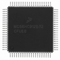
MCHC912B32CFUE8 Freescale Semiconductor, MCHC912B32CFUE8 Datasheet - Page 204

MCHC912B32CFUE8
Manufacturer Part Number
MCHC912B32CFUE8
Description
IC MCU 32K FLASH 8MHZ 80-QFP
Manufacturer
Freescale Semiconductor
Series
HC12r
Datasheet
1.MCHC912B32CFUE8.pdf
(334 pages)
Specifications of MCHC912B32CFUE8
Core Processor
CPU12
Core Size
16-Bit
Speed
8MHz
Connectivity
SCI, SPI
Peripherals
POR, PWM, WDT
Number Of I /o
63
Program Memory Size
32KB (32K x 8)
Program Memory Type
FLASH
Eeprom Size
768 x 8
Ram Size
1K x 8
Voltage - Supply (vcc/vdd)
4.5 V ~ 5.5 V
Data Converters
A/D 8x10b
Oscillator Type
External
Operating Temperature
-40°C ~ 85°C
Package / Case
80-QFP
Cpu Family
HC12
Device Core Size
16b
Frequency (max)
8MHz
Interface Type
SCI/SPI
Total Internal Ram Size
1KB
# I/os (max)
63
Operating Supply Voltage (typ)
5V
Operating Supply Voltage (max)
5.5V
Operating Supply Voltage (min)
4.5V
On-chip Adc
8-chx10-bit
Instruction Set Architecture
CISC
Operating Temp Range
-40C to 85C
Operating Temperature Classification
Industrial
Mounting
Surface Mount
Pin Count
80
Package Type
PQFP
Package
80PQFP
Family Name
HC12
Maximum Speed
8 MHz
Operating Supply Voltage
5 V
Data Bus Width
16 Bit
Number Of Programmable I/os
63
Processor Series
HC912B
Core
HC12
Data Ram Size
1 KB
Maximum Clock Frequency
8 MHz
Maximum Operating Temperature
+ 85 C
Mounting Style
SMD/SMT
3rd Party Development Tools
EWHCS12
Development Tools By Supplier
M68EVB912B32E
Minimum Operating Temperature
- 40 C
Lead Free Status / RoHS Status
Lead free / RoHS Compliant
Available stocks
Company
Part Number
Manufacturer
Quantity
Price
Company:
Part Number:
MCHC912B32CFUE8
Manufacturer:
Freescale Semiconductor
Quantity:
10 000
- Current page: 204 of 334
- Download datasheet (2Mb)
Serial Interface
14.3.4 Bidirectional Mode (MOMI or SISO)
In bidirectional mode, the SPI uses only one serial data pin for external device interface. The MSTR bit
decides which pin to be used. The MOSI pin becomes a serial data I/O (MOMI) pin for the master mode,
and the MISO pin becomes a serial data I/O (SISO) pin for the slave mode. The direction of each serial
I/O pin depends on the corresponding DDRS bit.
14.3.5 SPI Register Descriptions
Control and data registers for the SPI subsystem are described in this section. The memory address
indicated for each register is the default address that is in use after reset. The entire 512-byte register
block can be mapped to any 2-Kbyte boundary within the standard 64-Kbyte address space. For more
information, refer to
14.3.5.1 SPI Control Register 1
Read: Anytime
Write: Anytime
SPIE — SPI Interrupt Enable Bit
204
When SPE = 1
Bidirectional
0 = SPI interrupts are inhibited.
1 = Hardware interrupt sequence is requested each time the SPIF or MODF status flag is set.
SPC0 = 0
SPC0 = 1
Normal
Mode
Mode
Address:
Reset:
Read:
Write:
Chapter 5 Operating Modes and Resource
SWOM enables open-drain output. PS4 becomes GPIO.
Serial Out
Serial Out
$00D0
Figure 14-14. Normal Mode and Bidirectional Mode
SPIE
Serial In
Serial In
Bit 7
SPI
SPI
0
Figure 14-15. SPI Control Register 1 (SP0CR1)
SWOM enables open-drain output.
Master Mode
SPE
MSTR = 1
M68HC12B Family Data Sheet, Rev. 9.1
DDS5
DDS5
6
0
SWOM
5
0
MOMI
PS4
MO
MI
MSTR
4
0
CPOL
SWOM enables open-drain output. PS5 becomes GPIO.
3
0
Mapping.
Serial Out
Serial Out
Serial In
Serial In
SPI
SPI
SWOM enables open-drain output.
CPHA
2
1
Slave Mode
MSTR = 0
DDS4
DDS4
SSOE
1
0
Freescale Semiconductor
LSBF
Bit 0
0
SISO
PS5
SO
SI
Related parts for MCHC912B32CFUE8
Image
Part Number
Description
Manufacturer
Datasheet
Request
R
Part Number:
Description:
Manufacturer:
Freescale Semiconductor, Inc
Datasheet:
Part Number:
Description:
Manufacturer:
Freescale Semiconductor, Inc
Datasheet:
Part Number:
Description:
Manufacturer:
Freescale Semiconductor, Inc
Datasheet:
Part Number:
Description:
Manufacturer:
Freescale Semiconductor, Inc
Datasheet:
Part Number:
Description:
Manufacturer:
Freescale Semiconductor, Inc
Datasheet:
Part Number:
Description:
Manufacturer:
Freescale Semiconductor, Inc
Datasheet:
Part Number:
Description:
Manufacturer:
Freescale Semiconductor, Inc
Datasheet:
Part Number:
Description:
Manufacturer:
Freescale Semiconductor, Inc
Datasheet:
Part Number:
Description:
Manufacturer:
Freescale Semiconductor, Inc
Datasheet:
Part Number:
Description:
Manufacturer:
Freescale Semiconductor, Inc
Datasheet:
Part Number:
Description:
Manufacturer:
Freescale Semiconductor, Inc
Datasheet:
Part Number:
Description:
Manufacturer:
Freescale Semiconductor, Inc
Datasheet:
Part Number:
Description:
Manufacturer:
Freescale Semiconductor, Inc
Datasheet:
Part Number:
Description:
Manufacturer:
Freescale Semiconductor, Inc
Datasheet:
Part Number:
Description:
Manufacturer:
Freescale Semiconductor, Inc
Datasheet:


