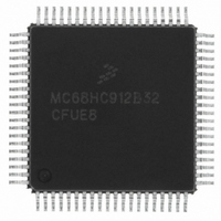
MCHC912B32CFUE8 Freescale Semiconductor, MCHC912B32CFUE8 Datasheet - Page 169

MCHC912B32CFUE8
Manufacturer Part Number
MCHC912B32CFUE8
Description
IC MCU 32K FLASH 8MHZ 80-QFP
Manufacturer
Freescale Semiconductor
Series
HC12r
Datasheet
1.MCHC912B32CFUE8.pdf
(334 pages)
Specifications of MCHC912B32CFUE8
Core Processor
CPU12
Core Size
16-Bit
Speed
8MHz
Connectivity
SCI, SPI
Peripherals
POR, PWM, WDT
Number Of I /o
63
Program Memory Size
32KB (32K x 8)
Program Memory Type
FLASH
Eeprom Size
768 x 8
Ram Size
1K x 8
Voltage - Supply (vcc/vdd)
4.5 V ~ 5.5 V
Data Converters
A/D 8x10b
Oscillator Type
External
Operating Temperature
-40°C ~ 85°C
Package / Case
80-QFP
Cpu Family
HC12
Device Core Size
16b
Frequency (max)
8MHz
Interface Type
SCI/SPI
Total Internal Ram Size
1KB
# I/os (max)
63
Operating Supply Voltage (typ)
5V
Operating Supply Voltage (max)
5.5V
Operating Supply Voltage (min)
4.5V
On-chip Adc
8-chx10-bit
Instruction Set Architecture
CISC
Operating Temp Range
-40C to 85C
Operating Temperature Classification
Industrial
Mounting
Surface Mount
Pin Count
80
Package Type
PQFP
Package
80PQFP
Family Name
HC12
Maximum Speed
8 MHz
Operating Supply Voltage
5 V
Data Bus Width
16 Bit
Number Of Programmable I/os
63
Processor Series
HC912B
Core
HC12
Data Ram Size
1 KB
Maximum Clock Frequency
8 MHz
Maximum Operating Temperature
+ 85 C
Mounting Style
SMD/SMT
3rd Party Development Tools
EWHCS12
Development Tools By Supplier
M68EVB912B32E
Minimum Operating Temperature
- 40 C
Lead Free Status / RoHS Status
Lead free / RoHS Compliant
Available stocks
Company
Part Number
Manufacturer
Quantity
Price
Company:
Part Number:
MCHC912B32CFUE8
Manufacturer:
Freescale Semiconductor
Quantity:
10 000
- Current page: 169 of 334
- Download datasheet (2Mb)
TSWAI — Timer Module Stops While in Wait Bit
TSBCK — Timer and Modulus Counter Stop While in Background Mode Bit
TFFCA — Timer Fast Flag Clear All Bit
13.4.7 Timer Control Registers
Read: Anytime
Write: Anytime
OMn Bits — Output Mode
OLn Bits — Output Level
Freescale Semiconductor
TSWAI also affects pulse accumulators and modulus down counters.
TBSCK does not stop the pulse accumulator.
These eight pairs of control bits are encoded to specify the output action to be taken as a result of a
successful OCn compare (see
becomes an output tied to OCn regardless of the state of the associated DDRT bit.
0 = Allows the timer module to continue running during wait
1 = Disables the timer module when the MCU is in wait mode. Timer interrupts cannot be used to
0 = Allows the timer and modulus counter to continue running while in background mode
1 = Disables the timer and modulus counter whenever the MCU is in background mode. This is
0 = Allows the timer flag clearing to function normally
1 = For TFLG1($8E), a read from an input capture or a write to the output compare channel
get the MCU out of wait.
useful for emulation.
($90–$9F) causes the corresponding channel flag, CnF, to be cleared. For TFLG2 ($8F), any
access to the TCNT register ($84, $85) clears the TOF flag. Any access to the PACN3 and
PACN2 registers ($A2, $A3) clears the PAOVF and PAIF flags in the PAFLG register ($A1).
Any access to the PACN1 and PACN0 registers ($A4, $A5) clears the PBOVF flag in the
PBFLG register ($B1). This has the advantage of eliminating software overhead in a separate
clear sequence. Extra care is required to avoid accidental flag clearing due to unintended
accesses.
Address: $0088
Address: $0089
To enable output action by OMn and OLn bits on the timer port, the
corresponding bit in OC7M should be cleared.
Reset:
Reset:
Read:
Read:
Write:
Write:
OM7
OM3
Bit 7
Bit 7
0
0
Figure 13-12. Timer Control Register 1 (TCTL1)
Figure 13-13. Timer Control Register 2 (TCTL2)
OL7
OL3
Table
6
0
6
0
M68HC12B Family Data Sheet, Rev. 9.1
13-1). When either OMn or OLn is 1, the pin associated with OCn
OM6
OM2
5
0
5
0
NOTE
OL6
OL2
4
0
4
0
OM5
OM1
3
0
3
0
OL5
OL1
2
0
2
0
OM4
OM0
1
0
1
0
Bit 0
Bit 0
OL4
OL0
0
0
Timer Registers
169
Related parts for MCHC912B32CFUE8
Image
Part Number
Description
Manufacturer
Datasheet
Request
R
Part Number:
Description:
Manufacturer:
Freescale Semiconductor, Inc
Datasheet:
Part Number:
Description:
Manufacturer:
Freescale Semiconductor, Inc
Datasheet:
Part Number:
Description:
Manufacturer:
Freescale Semiconductor, Inc
Datasheet:
Part Number:
Description:
Manufacturer:
Freescale Semiconductor, Inc
Datasheet:
Part Number:
Description:
Manufacturer:
Freescale Semiconductor, Inc
Datasheet:
Part Number:
Description:
Manufacturer:
Freescale Semiconductor, Inc
Datasheet:
Part Number:
Description:
Manufacturer:
Freescale Semiconductor, Inc
Datasheet:
Part Number:
Description:
Manufacturer:
Freescale Semiconductor, Inc
Datasheet:
Part Number:
Description:
Manufacturer:
Freescale Semiconductor, Inc
Datasheet:
Part Number:
Description:
Manufacturer:
Freescale Semiconductor, Inc
Datasheet:
Part Number:
Description:
Manufacturer:
Freescale Semiconductor, Inc
Datasheet:
Part Number:
Description:
Manufacturer:
Freescale Semiconductor, Inc
Datasheet:
Part Number:
Description:
Manufacturer:
Freescale Semiconductor, Inc
Datasheet:
Part Number:
Description:
Manufacturer:
Freescale Semiconductor, Inc
Datasheet:
Part Number:
Description:
Manufacturer:
Freescale Semiconductor, Inc
Datasheet:


