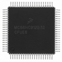
MCHC912B32CFUE8 Freescale Semiconductor, MCHC912B32CFUE8 Datasheet - Page 247

MCHC912B32CFUE8
Manufacturer Part Number
MCHC912B32CFUE8
Description
IC MCU 32K FLASH 8MHZ 80-QFP
Manufacturer
Freescale Semiconductor
Series
HC12r
Datasheet
1.MCHC912B32CFUE8.pdf
(334 pages)
Specifications of MCHC912B32CFUE8
Core Processor
CPU12
Core Size
16-Bit
Speed
8MHz
Connectivity
SCI, SPI
Peripherals
POR, PWM, WDT
Number Of I /o
63
Program Memory Size
32KB (32K x 8)
Program Memory Type
FLASH
Eeprom Size
768 x 8
Ram Size
1K x 8
Voltage - Supply (vcc/vdd)
4.5 V ~ 5.5 V
Data Converters
A/D 8x10b
Oscillator Type
External
Operating Temperature
-40°C ~ 85°C
Package / Case
80-QFP
Cpu Family
HC12
Device Core Size
16b
Frequency (max)
8MHz
Interface Type
SCI/SPI
Total Internal Ram Size
1KB
# I/os (max)
63
Operating Supply Voltage (typ)
5V
Operating Supply Voltage (max)
5.5V
Operating Supply Voltage (min)
4.5V
On-chip Adc
8-chx10-bit
Instruction Set Architecture
CISC
Operating Temp Range
-40C to 85C
Operating Temperature Classification
Industrial
Mounting
Surface Mount
Pin Count
80
Package Type
PQFP
Package
80PQFP
Family Name
HC12
Maximum Speed
8 MHz
Operating Supply Voltage
5 V
Data Bus Width
16 Bit
Number Of Programmable I/os
63
Processor Series
HC912B
Core
HC12
Data Ram Size
1 KB
Maximum Clock Frequency
8 MHz
Maximum Operating Temperature
+ 85 C
Mounting Style
SMD/SMT
3rd Party Development Tools
EWHCS12
Development Tools By Supplier
M68EVB912B32E
Minimum Operating Temperature
- 40 C
Lead Free Status / RoHS Status
Lead free / RoHS Compliant
Available stocks
Company
Part Number
Manufacturer
Quantity
Price
Company:
Part Number:
MCHC912B32CFUE8
Manufacturer:
Freescale Semiconductor
Quantity:
10 000
- Current page: 247 of 334
- Download datasheet (2Mb)
When a high priority message is scheduled by the application software, it may become necessary to abort
a lower priority message being set up in one of the three transmit buffers. Because messages that are
already under transmission cannot be aborted, the user has to request the abort by setting the
corresponding abort request flag (ABTRQ) in the transmission control register (CTCR). The msCAN12
grants the request, if possible, by setting the corresponding abort request acknowledge (ABTAK) and the
TXE flag to release the buffer and by generating a transmit interrupt. The transmit interrupt handler
software can tell from the setting of the ABTAK flag whether the message was aborted (ABTAK = 1)
or sent in the meantime (ABTAK = 0).
16.4 Identifier Acceptance Filter
The identifier acceptance registers (CIDAR0–CIADAR7) define the acceptable patterns of the standard
or extended identifier (ID10–ID0 or ID28–ID0). Any of these bits can be marked don’t care in the identifier
mask registers (CIDMR0–CIDMR7).
A filter hit is indicated to the application software by:
These identifier hit flags (IDHIT2–IDHIT0) clearly identify the filter section that caused the acceptance.
They simplify the application software’s task to identify the cause of the receiver interrupt. When more
than one hit occurs (two or more filters match), the lower hit has priority.
A flexible, programmable generic identifier acceptance filter has been introduced to reduce the CPU
interrupt loading. The filter is programmable to operate in four different modes:
Freescale Semiconductor
1. Two identifier acceptance filters, each to be applied to the full 29 bits of the identifier and to three
•
•
A set RXF (receive buffer full flag)
See
Three bits in the identifier acceptance control register
See
bits of the CAN frame: RTR, IDE, and SRR. This mode implements two filters for a full length CAN
2.0B compliant extended identifier.
(CIDAR0–CIDAR3, CIDMR0–CIDMR3) produces a filter 0 hit. Similarly, the second filter bank
(CIDAR4–CUIDAR7, CIDMR4–CIDMR7) produces a filter 1 hit.
16.12.5 msCAN12 Receiver Flag
16.12.9 msCAN12 Identifier Acceptance Control
ID28
ID10
AC7
AC7
CIDMRO
Figure 16-3. 32-Bit Maskable Identifier Acceptance Filter
CIDARO
IDR0
IDR0
ID21 ID20
AC0 AC7
AC0 AC7
ID3 ID2
M68HC12B Family Data Sheet, Rev. 9.1
CIDMR1
CIDAR1
IDR1
IDR1
ID accepted (Filter 0 hit)
Figure 16-3
IDE
Register) and
ID15 ID14
AC0 AC7
AC0 AC7
shows how the first 32-bit filter bank
CIDMR2
CIDAR2
IDR2
Register).
AC0
AC0
ID7
ID6
AC7
AC7
CIDMR3
CIDAR3
IDR3
Identifier Acceptance Filter
RTR
AC0
AC0
247
Related parts for MCHC912B32CFUE8
Image
Part Number
Description
Manufacturer
Datasheet
Request
R
Part Number:
Description:
Manufacturer:
Freescale Semiconductor, Inc
Datasheet:
Part Number:
Description:
Manufacturer:
Freescale Semiconductor, Inc
Datasheet:
Part Number:
Description:
Manufacturer:
Freescale Semiconductor, Inc
Datasheet:
Part Number:
Description:
Manufacturer:
Freescale Semiconductor, Inc
Datasheet:
Part Number:
Description:
Manufacturer:
Freescale Semiconductor, Inc
Datasheet:
Part Number:
Description:
Manufacturer:
Freescale Semiconductor, Inc
Datasheet:
Part Number:
Description:
Manufacturer:
Freescale Semiconductor, Inc
Datasheet:
Part Number:
Description:
Manufacturer:
Freescale Semiconductor, Inc
Datasheet:
Part Number:
Description:
Manufacturer:
Freescale Semiconductor, Inc
Datasheet:
Part Number:
Description:
Manufacturer:
Freescale Semiconductor, Inc
Datasheet:
Part Number:
Description:
Manufacturer:
Freescale Semiconductor, Inc
Datasheet:
Part Number:
Description:
Manufacturer:
Freescale Semiconductor, Inc
Datasheet:
Part Number:
Description:
Manufacturer:
Freescale Semiconductor, Inc
Datasheet:
Part Number:
Description:
Manufacturer:
Freescale Semiconductor, Inc
Datasheet:
Part Number:
Description:
Manufacturer:
Freescale Semiconductor, Inc
Datasheet:


