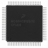
MCHC912B32CFUE8 Freescale Semiconductor, MCHC912B32CFUE8 Datasheet - Page 143

MCHC912B32CFUE8
Manufacturer Part Number
MCHC912B32CFUE8
Description
IC MCU 32K FLASH 8MHZ 80-QFP
Manufacturer
Freescale Semiconductor
Series
HC12r
Datasheet
1.MCHC912B32CFUE8.pdf
(334 pages)
Specifications of MCHC912B32CFUE8
Core Processor
CPU12
Core Size
16-Bit
Speed
8MHz
Connectivity
SCI, SPI
Peripherals
POR, PWM, WDT
Number Of I /o
63
Program Memory Size
32KB (32K x 8)
Program Memory Type
FLASH
Eeprom Size
768 x 8
Ram Size
1K x 8
Voltage - Supply (vcc/vdd)
4.5 V ~ 5.5 V
Data Converters
A/D 8x10b
Oscillator Type
External
Operating Temperature
-40°C ~ 85°C
Package / Case
80-QFP
Cpu Family
HC12
Device Core Size
16b
Frequency (max)
8MHz
Interface Type
SCI/SPI
Total Internal Ram Size
1KB
# I/os (max)
63
Operating Supply Voltage (typ)
5V
Operating Supply Voltage (max)
5.5V
Operating Supply Voltage (min)
4.5V
On-chip Adc
8-chx10-bit
Instruction Set Architecture
CISC
Operating Temp Range
-40C to 85C
Operating Temperature Classification
Industrial
Mounting
Surface Mount
Pin Count
80
Package Type
PQFP
Package
80PQFP
Family Name
HC12
Maximum Speed
8 MHz
Operating Supply Voltage
5 V
Data Bus Width
16 Bit
Number Of Programmable I/os
63
Processor Series
HC912B
Core
HC12
Data Ram Size
1 KB
Maximum Clock Frequency
8 MHz
Maximum Operating Temperature
+ 85 C
Mounting Style
SMD/SMT
3rd Party Development Tools
EWHCS12
Development Tools By Supplier
M68EVB912B32E
Minimum Operating Temperature
- 40 C
Lead Free Status / RoHS Status
Lead free / RoHS Compliant
Available stocks
Company
Part Number
Manufacturer
Quantity
Price
Company:
Part Number:
MCHC912B32CFUE8
Manufacturer:
Freescale Semiconductor
Quantity:
10 000
- Current page: 143 of 334
- Download datasheet (2Mb)
12.3.1 Timer Compare Force Register
Read: Anytime, always returns $00 (1 state is transient)
Write: Anytime
FOC7–FOC0 — Force Output Compare Action Bits for Channels 7–0
12.3.2 Output Compare 7 Mask Register
Read: Anytime
Write: Anytime
The bits of OC7M correspond bit-for-bit with the bits of the timer port (PORTT). Setting the OC7Mn sets
the corresponding port to be an output port regardless of the state of the DDRTn bit when the
corresponding TIOSn bit is set to be an output compare. This does not change the state of the DDRT bits.
12.3.3 Output Compare 7 Data Register
Read: Anytime
Write: Anytime
The bits of OC7D correspond bit-for-bit with the bits of the timer port (PORTT). When a successful OC7
compare occurs, for each bit that is set in OC7M, the corresponding data bit in OC7D is stored to the
corresponding bit of the timer port.
When the OC7Mn bit is set, a successful OC7 action will override a successful OC6–OC0 compare action
during the same cycle; therefore, the OCn action taken will depend on the corresponding OC7D bit.
Freescale Semiconductor
A write to this register with the corresponding data bit(s) set causes the action which is programmed
for output compare n to occur immediately. The action taken is the same as if a successful comparison
had just taken place with the TCn register except that the interrupt flag does not get set.
Address: $0081
Address: $0082
Address: $0083
Reset:
Reset:
Reset:
Read:
Read:
Read:
Write:
Write:
Write:
OC7M7
OC7D7
Figure 12-4. Output Compare 7 Mask Register (OC7M)
FOC7
Figure 12-3. Timer Compare Force Register (CFORC)
Figure 12-5. Output Compare 7 Data Register (OC7D)
Bit 7
Bit 7
Bit 7
0
0
0
OC7M6
OC7D6
FOC6
6
0
6
0
6
0
M68HC12B Family Data Sheet, Rev. 9.1
OC7M5
OC7D5
FOC5
5
0
5
0
5
0
OC7M4
OC7D4
FOC4
4
0
4
0
4
0
OC7M3
OC7D3
FOC3
3
0
3
0
3
0
OC7M2
OC7D2
FOC2
2
0
2
0
2
0
OC7M1
OC7D1
FOC1
1
0
1
0
1
0
OC7M0
OC7D0
FOC0
Bit 0
Bit 0
Bit 0
0
0
0
Block Diagram
143
Related parts for MCHC912B32CFUE8
Image
Part Number
Description
Manufacturer
Datasheet
Request
R
Part Number:
Description:
Manufacturer:
Freescale Semiconductor, Inc
Datasheet:
Part Number:
Description:
Manufacturer:
Freescale Semiconductor, Inc
Datasheet:
Part Number:
Description:
Manufacturer:
Freescale Semiconductor, Inc
Datasheet:
Part Number:
Description:
Manufacturer:
Freescale Semiconductor, Inc
Datasheet:
Part Number:
Description:
Manufacturer:
Freescale Semiconductor, Inc
Datasheet:
Part Number:
Description:
Manufacturer:
Freescale Semiconductor, Inc
Datasheet:
Part Number:
Description:
Manufacturer:
Freescale Semiconductor, Inc
Datasheet:
Part Number:
Description:
Manufacturer:
Freescale Semiconductor, Inc
Datasheet:
Part Number:
Description:
Manufacturer:
Freescale Semiconductor, Inc
Datasheet:
Part Number:
Description:
Manufacturer:
Freescale Semiconductor, Inc
Datasheet:
Part Number:
Description:
Manufacturer:
Freescale Semiconductor, Inc
Datasheet:
Part Number:
Description:
Manufacturer:
Freescale Semiconductor, Inc
Datasheet:
Part Number:
Description:
Manufacturer:
Freescale Semiconductor, Inc
Datasheet:
Part Number:
Description:
Manufacturer:
Freescale Semiconductor, Inc
Datasheet:
Part Number:
Description:
Manufacturer:
Freescale Semiconductor, Inc
Datasheet:


