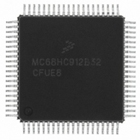
MCHC912B32CFUE8 Freescale Semiconductor, MCHC912B32CFUE8 Datasheet - Page 192

MCHC912B32CFUE8
Manufacturer Part Number
MCHC912B32CFUE8
Description
IC MCU 32K FLASH 8MHZ 80-QFP
Manufacturer
Freescale Semiconductor
Series
HC12r
Datasheet
1.MCHC912B32CFUE8.pdf
(334 pages)
Specifications of MCHC912B32CFUE8
Core Processor
CPU12
Core Size
16-Bit
Speed
8MHz
Connectivity
SCI, SPI
Peripherals
POR, PWM, WDT
Number Of I /o
63
Program Memory Size
32KB (32K x 8)
Program Memory Type
FLASH
Eeprom Size
768 x 8
Ram Size
1K x 8
Voltage - Supply (vcc/vdd)
4.5 V ~ 5.5 V
Data Converters
A/D 8x10b
Oscillator Type
External
Operating Temperature
-40°C ~ 85°C
Package / Case
80-QFP
Cpu Family
HC12
Device Core Size
16b
Frequency (max)
8MHz
Interface Type
SCI/SPI
Total Internal Ram Size
1KB
# I/os (max)
63
Operating Supply Voltage (typ)
5V
Operating Supply Voltage (max)
5.5V
Operating Supply Voltage (min)
4.5V
On-chip Adc
8-chx10-bit
Instruction Set Architecture
CISC
Operating Temp Range
-40C to 85C
Operating Temperature Classification
Industrial
Mounting
Surface Mount
Pin Count
80
Package Type
PQFP
Package
80PQFP
Family Name
HC12
Maximum Speed
8 MHz
Operating Supply Voltage
5 V
Data Bus Width
16 Bit
Number Of Programmable I/os
63
Processor Series
HC912B
Core
HC12
Data Ram Size
1 KB
Maximum Clock Frequency
8 MHz
Maximum Operating Temperature
+ 85 C
Mounting Style
SMD/SMT
3rd Party Development Tools
EWHCS12
Development Tools By Supplier
M68EVB912B32E
Minimum Operating Temperature
- 40 C
Lead Free Status / RoHS Status
Lead free / RoHS Compliant
Available stocks
Company
Part Number
Manufacturer
Quantity
Price
Company:
Part Number:
MCHC912B32CFUE8
Manufacturer:
Freescale Semiconductor
Quantity:
10 000
- Current page: 192 of 334
- Download datasheet (2Mb)
Serial Interface
14.2 Serial Communication Interface (SCI)
The SCI on the MCU is an NRZ format (one start, eight or nine data, and one stop bit) asynchronous
communication system with independent internal baud rate generation circuitry and an SCI transmitter
and receiver. It can be configured for eight or nine data bits (one of which may be designated as a parity
bit, odd or even). If enabled, parity is generated in hardware for transmitted and received data. Receiver
parity errors are flagged in hardware. The baud rate generator is based on a modulus counter, allowing
flexibility in choosing baud rates. There is a receiver wakeup feature, an idle line detect feature, a
loop-back mode, and various error detection features. Two port pins provide the external interface for the
transmitted data (TXD) and the received data (RXD). See
192
INTERNAL
LOGIC
TO
DATA BUS
Figure 14-2. Serial Communications Interface Block Diagram
SC0BD/SELECT
DIVIDER
MCLK
DETECT
PARITY
SC0CR1/SCI CTL 1
BAUD RATE
M68HC12B Family Data Sheet, Rev. 9.1
TX BAUD RATE
CLOCK
RX BAUD RATE
INT REQUEST LOGIC
SC0SR1/INT STATUS
SC0CR1/SCI CTL 1
DATA RECOVERY
INT REQUEST LOGIC
GENERATOR
PARITY
WAKEUP LOGIC
Figure
MSB
MSB
RxD BUFFER/SC0DRL
10-11 BIT SHIFT REG
TxD BUFFER/SC0DRL
SC0SR1/INT STATUS
10-11 BIT SHIFT REG
SC0CR2/SCI CTL 2
SC0CR2/SCI CTL 2
14-2.
SCI TRANSMITTER
TxMTR CONTROL
SCI RECEIVER
LSB
LSB
Freescale Semiconductor
PS1
RxD
TxD
PS0
Related parts for MCHC912B32CFUE8
Image
Part Number
Description
Manufacturer
Datasheet
Request
R
Part Number:
Description:
Manufacturer:
Freescale Semiconductor, Inc
Datasheet:
Part Number:
Description:
Manufacturer:
Freescale Semiconductor, Inc
Datasheet:
Part Number:
Description:
Manufacturer:
Freescale Semiconductor, Inc
Datasheet:
Part Number:
Description:
Manufacturer:
Freescale Semiconductor, Inc
Datasheet:
Part Number:
Description:
Manufacturer:
Freescale Semiconductor, Inc
Datasheet:
Part Number:
Description:
Manufacturer:
Freescale Semiconductor, Inc
Datasheet:
Part Number:
Description:
Manufacturer:
Freescale Semiconductor, Inc
Datasheet:
Part Number:
Description:
Manufacturer:
Freescale Semiconductor, Inc
Datasheet:
Part Number:
Description:
Manufacturer:
Freescale Semiconductor, Inc
Datasheet:
Part Number:
Description:
Manufacturer:
Freescale Semiconductor, Inc
Datasheet:
Part Number:
Description:
Manufacturer:
Freescale Semiconductor, Inc
Datasheet:
Part Number:
Description:
Manufacturer:
Freescale Semiconductor, Inc
Datasheet:
Part Number:
Description:
Manufacturer:
Freescale Semiconductor, Inc
Datasheet:
Part Number:
Description:
Manufacturer:
Freescale Semiconductor, Inc
Datasheet:
Part Number:
Description:
Manufacturer:
Freescale Semiconductor, Inc
Datasheet:


