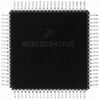
MC9S12C64CFUE Freescale Semiconductor, MC9S12C64CFUE Datasheet - Page 173

MC9S12C64CFUE
Manufacturer Part Number
MC9S12C64CFUE
Description
IC MCU 64K FLASH 4K RAM 80-QFP
Manufacturer
Freescale Semiconductor
Series
HCS12r
Specifications of MC9S12C64CFUE
Core Processor
HCS12
Core Size
16-Bit
Speed
25MHz
Connectivity
CAN, EBI/EMI, SCI, SPI
Peripherals
POR, PWM, WDT
Number Of I /o
60
Program Memory Size
64KB (64K x 8)
Program Memory Type
FLASH
Ram Size
4K x 8
Voltage - Supply (vcc/vdd)
2.35 V ~ 5.5 V
Data Converters
A/D 8x10b
Oscillator Type
Internal
Operating Temperature
-40°C ~ 85°C
Package / Case
80-QFP
Processor Series
S12C
Core
HCS12
Data Bus Width
16 bit
Data Ram Size
4 KB
Interface Type
CAN/SCI/SPI
Maximum Clock Frequency
25 MHz
Number Of Programmable I/os
60
Number Of Timers
8
Maximum Operating Temperature
+ 85 C
Mounting Style
SMD/SMT
3rd Party Development Tools
EWHCS12
Development Tools By Supplier
M68EVB912C32EE
Minimum Operating Temperature
- 40 C
On-chip Adc
8-ch x 10-bit
Package
80PQFP
Family Name
HCS12
Maximum Speed
25 MHz
Operating Supply Voltage
2.5|5 V
Height
2.4 mm
Length
14 mm
Supply Voltage (max)
2.75 V, 5.5 V
Supply Voltage (min)
2.35 V, 2.97 V
Width
14 mm
Lead Free Status / RoHS Status
Lead free / RoHS Compliant
Eeprom Size
-
Lead Free Status / Rohs Status
Lead free / RoHS Compliant
Available stocks
Company
Part Number
Manufacturer
Quantity
Price
Company:
Part Number:
MC9S12C64CFUE
Manufacturer:
Freescale Semiconductor
Quantity:
10 000
- Current page: 173 of 690
- Download datasheet (4Mb)
6.3.2.2
Read: All modes
Write: All modes
When entering background debug mode, the BDM CCR holding register is used to save the contents of the
condition code register of the user’s program. It is also used for temporary storage in the standard BDM
firmware mode. The BDM CCR holding register can be written to modify the CCR value.
6.3.2.3
Read: All modes
Write: Never
Freescale Semiconductor
0xFF06
0xFF07
REG[14:11]
Reset
Reset
Field
6:3
W
W
R
R
CCR7
Internal Register Map Position — These four bits show the state of the upper five bits of the base address for
the system’s relocatable register block. BDMINR is a shadow of the INITRG register which maps the register
block to any 2K byte space within the first 32K bytes of the 64K byte address space.
BDM CCR Holding Register (BDMCCR)
BDM Internal Register Position Register (BDMINR)
0
0
0
7
7
When BDM is made active, the CPU stores the value of the CCR register in
the BDMCCR register. However, out of special single-chip reset, the
BDMCCR is set to 0xD8 and not 0xD0 which is the reset value of the CCR
register.
= Unimplemented or Reserved
REG14
CCR6
0
0
6
6
Figure 6-5. BDM Internal Register Position (BDMINR)
Figure 6-4. BDM CCR Holding Register (BDMCCR)
Table 6-4. BDMINR Field Descriptions
REG13
CCR5
MC9S12C-Family / MC9S12GC-Family
0
0
5
5
REG12
CCR4
Rev 01.24
NOTE
0
0
4
4
Chapter 6 Background Debug Module (BDMV4) Block Description
Description
REG11
CCR3
0
0
3
3
CCR2
0
0
0
2
2
CCR1
0
0
0
1
1
CCR0
0
0
0
0
0
173
Related parts for MC9S12C64CFUE
Image
Part Number
Description
Manufacturer
Datasheet
Request
R
Part Number:
Description:
Manufacturer:
Freescale Semiconductor, Inc
Datasheet:
Part Number:
Description:
Manufacturer:
Freescale Semiconductor, Inc
Datasheet:
Part Number:
Description:
Manufacturer:
Freescale Semiconductor, Inc
Datasheet:
Part Number:
Description:
Manufacturer:
Freescale Semiconductor, Inc
Datasheet:
Part Number:
Description:
Manufacturer:
Freescale Semiconductor, Inc
Datasheet:
Part Number:
Description:
Manufacturer:
Freescale Semiconductor, Inc
Datasheet:
Part Number:
Description:
Manufacturer:
Freescale Semiconductor, Inc
Datasheet:
Part Number:
Description:
Manufacturer:
Freescale Semiconductor, Inc
Datasheet:
Part Number:
Description:
Manufacturer:
Freescale Semiconductor, Inc
Datasheet:
Part Number:
Description:
Manufacturer:
Freescale Semiconductor, Inc
Datasheet:
Part Number:
Description:
Manufacturer:
Freescale Semiconductor, Inc
Datasheet:
Part Number:
Description:
Manufacturer:
Freescale Semiconductor, Inc
Datasheet:
Part Number:
Description:
Manufacturer:
Freescale Semiconductor, Inc
Datasheet:
Part Number:
Description:
Manufacturer:
Freescale Semiconductor, Inc
Datasheet:
Part Number:
Description:
Manufacturer:
Freescale Semiconductor, Inc
Datasheet:


