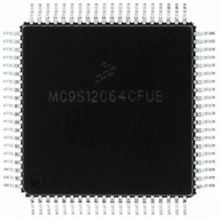
MC9S12C64CFUE Freescale Semiconductor, MC9S12C64CFUE Datasheet - Page 53

MC9S12C64CFUE
Manufacturer Part Number
MC9S12C64CFUE
Description
IC MCU 64K FLASH 4K RAM 80-QFP
Manufacturer
Freescale Semiconductor
Series
HCS12r
Specifications of MC9S12C64CFUE
Core Processor
HCS12
Core Size
16-Bit
Speed
25MHz
Connectivity
CAN, EBI/EMI, SCI, SPI
Peripherals
POR, PWM, WDT
Number Of I /o
60
Program Memory Size
64KB (64K x 8)
Program Memory Type
FLASH
Ram Size
4K x 8
Voltage - Supply (vcc/vdd)
2.35 V ~ 5.5 V
Data Converters
A/D 8x10b
Oscillator Type
Internal
Operating Temperature
-40°C ~ 85°C
Package / Case
80-QFP
Processor Series
S12C
Core
HCS12
Data Bus Width
16 bit
Data Ram Size
4 KB
Interface Type
CAN/SCI/SPI
Maximum Clock Frequency
25 MHz
Number Of Programmable I/os
60
Number Of Timers
8
Maximum Operating Temperature
+ 85 C
Mounting Style
SMD/SMT
3rd Party Development Tools
EWHCS12
Development Tools By Supplier
M68EVB912C32EE
Minimum Operating Temperature
- 40 C
On-chip Adc
8-ch x 10-bit
Package
80PQFP
Family Name
HCS12
Maximum Speed
25 MHz
Operating Supply Voltage
2.5|5 V
Height
2.4 mm
Length
14 mm
Supply Voltage (max)
2.75 V, 5.5 V
Supply Voltage (min)
2.35 V, 2.97 V
Width
14 mm
Lead Free Status / RoHS Status
Lead free / RoHS Compliant
Eeprom Size
-
Lead Free Status / Rohs Status
Lead free / RoHS Compliant
Available stocks
Company
Part Number
Manufacturer
Quantity
Price
Company:
Part Number:
MC9S12C64CFUE
Manufacturer:
Freescale Semiconductor
Quantity:
10 000
- Current page: 53 of 690
- Download datasheet (4Mb)
1.3.4.13
In all modes this pin can be used as a general-purpose I/O and is an input with an active pull-up out of
reset. If the read/write function is required it should be enabled by setting the RDWE bit in the PEAR
register. External writes will not be possible until enabled. This pin is not available in the 48- / 52-pin
package versions.
1.3.4.14
The IRQ input provides a means of applying asynchronous interrupt requests to the MCU. Either falling
edge-sensitive triggering or level-sensitive triggering is program selectable (INTCR register). IRQ is
always enabled and configured to level-sensitive triggering out of reset. It can be disabled by clearing
IRQEN bit (INTCR register). When the MCU is reset the IRQ function is masked in the condition code
register. This pin is always an input and can always be read. There is an active pull-up on this pin while in
reset and immediately out of reset. The pull-up can be turned off by clearing PUPEE in the PUCR register.
1.3.4.15
The XIRQ input provides a means of requesting a non-maskable interrupt after reset initialization. During
reset, the X bit in the condition code register (CCR) is set and any interrupt is masked until MCU software
enables it. Because the XIRQ input is level sensitive, it can be connected to a multiple-source wired-OR
network. This pin is always an input and can always be read. There is an active pull-up on this pin while
in reset and immediately out of reset. The pull-up can be turned off by clearing PUPEE in the PUCR
register.
1.3.4.16
PAD7–PAD0 are general purpose I/O pins and also analog inputs for the analog to digital converter. In
order to use a PAD pin as a standard input, the corresponding ATDDIEN register bit must be set. These
bits are cleared out of reset to configure the PAD pins for A/D operation.
When the A/D converter is active in multi-channel mode, port inputs are scanned and converted
irrespective of Port AD configuration. Thus Port AD pins that are configured as digital inputs or digital
outputs are also converted in the A/D conversion sequence.
1.3.4.17
PP7 is a general purpose input or output pin, shared with the keypad interrupt function. When configured
as an input, it can generate interrupts causing the MCU to exit stop or wait mode. This pin is not available
in the 48- / 52-pin package versions.
1.3.4.18
PP6 is a general purpose input or output pin, shared with the keypad interrupt function. When configured
as an input, it can generate interrupts causing the MCU to exit stop or wait mode. This pin is not available
in the 48- / 52-pin package versions. During MCU expanded modes of operation, this pin is used to enable
Freescale Semiconductor
PE2 / R/W — Port E I/O Pin [2] / Read/Write
PE1 / IRQ — Port E Input Pin [1] / Maskable Interrupt Pin
PE0 / XIRQ — Port E input Pin [0] / Non Maskable Interrupt Pin
PAD[7:0] / AN[7:0] — Port AD I/O Pins [7:0]
PP[7] / KWP[7] — Port P I/O Pin [7]
PP[6] / KWP[6]/ROMCTL — Port P I/O Pin [6]
MC9S12C-Family / MC9S12GC-Family
Rev 01.24
Chapter 1 MC9S12C and MC9S12GC Device Overview (MC9S12C128)
53
Related parts for MC9S12C64CFUE
Image
Part Number
Description
Manufacturer
Datasheet
Request
R
Part Number:
Description:
Manufacturer:
Freescale Semiconductor, Inc
Datasheet:
Part Number:
Description:
Manufacturer:
Freescale Semiconductor, Inc
Datasheet:
Part Number:
Description:
Manufacturer:
Freescale Semiconductor, Inc
Datasheet:
Part Number:
Description:
Manufacturer:
Freescale Semiconductor, Inc
Datasheet:
Part Number:
Description:
Manufacturer:
Freescale Semiconductor, Inc
Datasheet:
Part Number:
Description:
Manufacturer:
Freescale Semiconductor, Inc
Datasheet:
Part Number:
Description:
Manufacturer:
Freescale Semiconductor, Inc
Datasheet:
Part Number:
Description:
Manufacturer:
Freescale Semiconductor, Inc
Datasheet:
Part Number:
Description:
Manufacturer:
Freescale Semiconductor, Inc
Datasheet:
Part Number:
Description:
Manufacturer:
Freescale Semiconductor, Inc
Datasheet:
Part Number:
Description:
Manufacturer:
Freescale Semiconductor, Inc
Datasheet:
Part Number:
Description:
Manufacturer:
Freescale Semiconductor, Inc
Datasheet:
Part Number:
Description:
Manufacturer:
Freescale Semiconductor, Inc
Datasheet:
Part Number:
Description:
Manufacturer:
Freescale Semiconductor, Inc
Datasheet:
Part Number:
Description:
Manufacturer:
Freescale Semiconductor, Inc
Datasheet:


