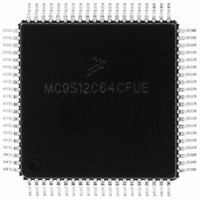
MC9S12C64CFUE Freescale Semiconductor, MC9S12C64CFUE Datasheet - Page 379

MC9S12C64CFUE
Manufacturer Part Number
MC9S12C64CFUE
Description
IC MCU 64K FLASH 4K RAM 80-QFP
Manufacturer
Freescale Semiconductor
Series
HCS12r
Specifications of MC9S12C64CFUE
Core Processor
HCS12
Core Size
16-Bit
Speed
25MHz
Connectivity
CAN, EBI/EMI, SCI, SPI
Peripherals
POR, PWM, WDT
Number Of I /o
60
Program Memory Size
64KB (64K x 8)
Program Memory Type
FLASH
Ram Size
4K x 8
Voltage - Supply (vcc/vdd)
2.35 V ~ 5.5 V
Data Converters
A/D 8x10b
Oscillator Type
Internal
Operating Temperature
-40°C ~ 85°C
Package / Case
80-QFP
Processor Series
S12C
Core
HCS12
Data Bus Width
16 bit
Data Ram Size
4 KB
Interface Type
CAN/SCI/SPI
Maximum Clock Frequency
25 MHz
Number Of Programmable I/os
60
Number Of Timers
8
Maximum Operating Temperature
+ 85 C
Mounting Style
SMD/SMT
3rd Party Development Tools
EWHCS12
Development Tools By Supplier
M68EVB912C32EE
Minimum Operating Temperature
- 40 C
On-chip Adc
8-ch x 10-bit
Package
80PQFP
Family Name
HCS12
Maximum Speed
25 MHz
Operating Supply Voltage
2.5|5 V
Height
2.4 mm
Length
14 mm
Supply Voltage (max)
2.75 V, 5.5 V
Supply Voltage (min)
2.35 V, 2.97 V
Width
14 mm
Lead Free Status / RoHS Status
Lead free / RoHS Compliant
Eeprom Size
-
Lead Free Status / Rohs Status
Lead free / RoHS Compliant
Available stocks
Company
Part Number
Manufacturer
Quantity
Price
Company:
Part Number:
MC9S12C64CFUE
Manufacturer:
Freescale Semiconductor
Quantity:
10 000
- Current page: 379 of 690
- Download datasheet (4Mb)
To calculate the output frequency in center aligned output mode for a particular channel, take the selected
clock source frequency for the channel (A, B, SA, or SB) and divide it by twice the value in the period
register for that channel.
As an example of a center aligned output, consider the following case:
Shown below is the output waveform generated.
12.4.2.7
The PWM timer also has the option of generating 6-channels of 8-bits or 3-channels of 16-bits for greater
PWM resolution}. This 16-bit channel option is achieved through the concatenation of two 8-bit channels.
The PWMCTL register contains three control bits, each of which is used to concatenate a pair of PWM
channels into one 16-bit channel. Channels 4 and 5 are concatenated with the CON45 bit, channels 2 and 3
are concatenated with the CON23 bit, and channels 0 and 1 are concatenated with the CON01 bit.
When channels 4 and 5 are concatenated, channel 4 registers become the high-order bytes of the double
byte channel as shown in
registers become the high-order bytes of the double byte channel. When channels 0 and 1 are concatenated,
channel 0 registers become the high-order bytes of the double byte channel.
Freescale Semiconductor
•
•
E = 100 ns
PWMx frequency = clock (A, B, SA, or SB) / (2*PWMPERx)
PWMx duty cycle (high time as a% of period):
— Polarity = 0 (PPOLx = 0)
— Polarity = 1 (PPOLx = 1)
Clock source = bus clock, where bus clock = 10 MHz (100 ns period)
PPOLx = 0
PWMPERx = 4
PWMDTYx = 1
PWMx frequency = 10 MHz/8 = 1.25 MHz
PWMx period = 800 ns
PWMx duty cycle = 3/4 *100% = 75%
Duty cycle = [(PWMPERx-PWMDTYx)/PWMPERx] * 100%
Duty cycle = [PWMDTYx / PWMPERx] * 100%
PWM 16-Bit Functions
Change these bits only when both corresponding channels are disabled.
Figure 12-39. PWM Center Aligned Output Example Waveform
Figure
12-40. Similarly, when channels 2 and 3 are concatenated, channel 2
MC9S12C-Family / MC9S12GC-Family
DUTY CYCLE = 75%
PERIOD = 800 ns
Rev 01.24
NOTE
Chapter 12 Pulse-Width Modulator (PWM8B6CV1) Block Description
E = 100 ns
379
Related parts for MC9S12C64CFUE
Image
Part Number
Description
Manufacturer
Datasheet
Request
R
Part Number:
Description:
Manufacturer:
Freescale Semiconductor, Inc
Datasheet:
Part Number:
Description:
Manufacturer:
Freescale Semiconductor, Inc
Datasheet:
Part Number:
Description:
Manufacturer:
Freescale Semiconductor, Inc
Datasheet:
Part Number:
Description:
Manufacturer:
Freescale Semiconductor, Inc
Datasheet:
Part Number:
Description:
Manufacturer:
Freescale Semiconductor, Inc
Datasheet:
Part Number:
Description:
Manufacturer:
Freescale Semiconductor, Inc
Datasheet:
Part Number:
Description:
Manufacturer:
Freescale Semiconductor, Inc
Datasheet:
Part Number:
Description:
Manufacturer:
Freescale Semiconductor, Inc
Datasheet:
Part Number:
Description:
Manufacturer:
Freescale Semiconductor, Inc
Datasheet:
Part Number:
Description:
Manufacturer:
Freescale Semiconductor, Inc
Datasheet:
Part Number:
Description:
Manufacturer:
Freescale Semiconductor, Inc
Datasheet:
Part Number:
Description:
Manufacturer:
Freescale Semiconductor, Inc
Datasheet:
Part Number:
Description:
Manufacturer:
Freescale Semiconductor, Inc
Datasheet:
Part Number:
Description:
Manufacturer:
Freescale Semiconductor, Inc
Datasheet:
Part Number:
Description:
Manufacturer:
Freescale Semiconductor, Inc
Datasheet:


