MC9S12C64CFUE Freescale Semiconductor, MC9S12C64CFUE Datasheet - Page 50
MC9S12C64CFUE
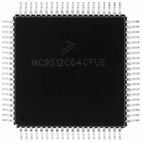
Manufacturer Part Number
MC9S12C64CFUE
Description
IC MCU 64K FLASH 4K RAM 80-QFP
Manufacturer
Freescale Semiconductor
Series
HCS12r
Specifications of MC9S12C64CFUE
Core Processor
HCS12
Core Size
16-Bit
Speed
25MHz
Connectivity
CAN, EBI/EMI, SCI, SPI
Peripherals
POR, PWM, WDT
Number Of I /o
60
Program Memory Size
64KB (64K x 8)
Program Memory Type
FLASH
Ram Size
4K x 8
Voltage - Supply (vcc/vdd)
2.35 V ~ 5.5 V
Data Converters
A/D 8x10b
Oscillator Type
Internal
Operating Temperature
-40°C ~ 85°C
Package / Case
80-QFP
Processor Series
S12C
Core
HCS12
Data Bus Width
16 bit
Data Ram Size
4 KB
Interface Type
CAN/SCI/SPI
Maximum Clock Frequency
25 MHz
Number Of Programmable I/os
60
Number Of Timers
8
Maximum Operating Temperature
+ 85 C
Mounting Style
SMD/SMT
3rd Party Development Tools
EWHCS12
Development Tools By Supplier
M68EVB912C32EE
Minimum Operating Temperature
- 40 C
On-chip Adc
8-ch x 10-bit
Package
80PQFP
Family Name
HCS12
Maximum Speed
25 MHz
Operating Supply Voltage
2.5|5 V
Height
2.4 mm
Length
14 mm
Supply Voltage (max)
2.75 V, 5.5 V
Supply Voltage (min)
2.35 V, 2.97 V
Width
14 mm
Lead Free Status / RoHS Status
Lead free / RoHS Compliant
Eeprom Size
-
Lead Free Status / Rohs Status
Lead free / RoHS Compliant
Available stocks
Company
Part Number
Manufacturer
Quantity
Price

Company:
Part Number:
MC9S12C64CFUE
Manufacturer:
Freescale Semiconductor
Quantity:
10 000


Chapter 1 MC9S12C and MC9S12GC Device Overview (MC9S12C128)
1.3.4
1.3.4.1
EXTAL and XTAL are the crystal driver and external clock pins. On reset all the device clocks are derived
from the EXTAL input frequency. XTAL is the crystal output.
1.3.4.2
RESET is an active low bidirectional control signal that acts as an input to initialize the MCU to a known
start-up state. It also acts as an open-drain output to indicate that an internal failure has been detected in
either the clock monitor or COP watchdog circuit. External circuitry connected to the RESET pin should
not include a large capacitance that would interfere with the ability of this signal to rise to a valid logic one
within 32 ECLK cycles after the low drive is released. Upon detection of any reset, an internal circuit
drives the RESET pin low and a clocked reset sequence controls when the MCU can begin normal
processing.
1.3.4.3
This pin is reserved for test and must be tied to V
1.3.4.4
Dedicated pin used to create the PLL loop filter. See CRG BUG for more detailed information.PLL loop
filter. Please ask your Motorola representative for the interactive application note to compute PLL loop
filter elements. Any current leakage on this pin must be avoided.
1.3.4.5
The BKGD / TAGHI / MODC pin is used as a pseudo-open-drain pin for the background debug
communication. In MCU expanded modes of operation when instruction tagging is on, an input low on
this pin during the falling edge of E-clock tags the high half of the instruction word being read into the
instruction queue. It is also used as a MCU operating mode select pin at the rising edge during reset, when
the state of this pin is latched to the MODC bit.
50
Detailed Signal Descriptions
EXTAL, XTAL — Oscillator Pins
RESET — External Reset Pin
TEST / V
XFC — PLL Loop Filter Pin
BKGD / TAGHI / MODC — Background Debug, Tag High, and Mode Pin
PP
— Test Pin
Figure 1-10. PLL Loop Filter Connections
MC9S12C-Family / MC9S12GC-Family
MCU
XFC
Rev 01.24
SS
V
DDPLL
in all applications.
R
C
0
S
V
DDPLL
C
P
Freescale Semiconductor
Related parts for MC9S12C64CFUE
Image
Part Number
Description
Manufacturer
Datasheet
Request
R

Part Number:
Description:
Manufacturer:
Freescale Semiconductor, Inc
Datasheet:
Part Number:
Description:
Manufacturer:
Freescale Semiconductor, Inc
Datasheet:
Part Number:
Description:
Manufacturer:
Freescale Semiconductor, Inc
Datasheet:
Part Number:
Description:
Manufacturer:
Freescale Semiconductor, Inc
Datasheet:
Part Number:
Description:
Manufacturer:
Freescale Semiconductor, Inc
Datasheet:
Part Number:
Description:
Manufacturer:
Freescale Semiconductor, Inc
Datasheet:
Part Number:
Description:
Manufacturer:
Freescale Semiconductor, Inc
Datasheet:
Part Number:
Description:
Manufacturer:
Freescale Semiconductor, Inc
Datasheet:
Part Number:
Description:
Manufacturer:
Freescale Semiconductor, Inc
Datasheet:
Part Number:
Description:
Manufacturer:
Freescale Semiconductor, Inc
Datasheet:
Part Number:
Description:
Manufacturer:
Freescale Semiconductor, Inc
Datasheet:
Part Number:
Description:
Manufacturer:
Freescale Semiconductor, Inc
Datasheet:
Part Number:
Description:
Manufacturer:
Freescale Semiconductor, Inc
Datasheet:
Part Number:
Description:
Manufacturer:
Freescale Semiconductor, Inc
Datasheet:
Part Number:
Description:
Manufacturer:
Freescale Semiconductor, Inc
Datasheet: