DS26518GN+ Maxim Integrated Products, DS26518GN+ Datasheet - Page 27
DS26518GN+
Manufacturer Part Number
DS26518GN+
Description
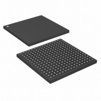
IC TXRX T1/E1/J1 8PORT 256-CSBGA
Manufacturer
Maxim Integrated Products
Type
Transceiverr
Specifications of DS26518GN+
Number Of Drivers/receivers
8/8
Protocol
T1/E1/J1
Voltage - Supply
3.135 V ~ 3.465 V
Mounting Type
Surface Mount
Package / Case
256-CSBGA
Lead Free Status / RoHS Status
Lead free / RoHS Compliant


SCANMODE
DVDD33
DVDD18
ARVDD
ACVDD
ATVDD
ARVSS
ACVSS
ATVSS
NAME
DVSS
G11, G12,
H10, H11
M1, M16,
M2, M15,
G1, G16,
G2, G15,
B1, B16,
K1, K16,
B2, B15,
K2, K15,
D1, D16,
E1, E16,
D2, D15,
E2, E15,
G7–G10
H12, J6,
R1, R16
R2, R15
N1, N16
N2, N15
G5, G6,
J8–J11,
K5–K12
H5, H6,
H8, H9,
H13
PIN
H7
J7
TYPE
Input
—
—
—
—
—
—
—
—
—
Scan Mode. When low, normal operational clocks are used to clock the flip flops.
User should tie low.
3.3V ±5% Analog Transmit Power Supply. These V
transmit LIU sections of the DS26518.
Analog Transmit V
3.3V ±5% Analog Receive Power Supply. These V
receive LIU sections of the DS26518.
Analog Receive V
1.8V ±5% Analog Clock Conversion V
conversion unit (CLAD) of the DS26518.
Analog Clock V
3.3V ±5% Power Supply for I/Os
1.8V ±5% Power Supply for Internal V
Digital Ground
POWER SUPPLIES
27 of 312
SS
. This pin is used for clock converter analog V
SS
SS
. These pins are used for analog V
. These pins are used for transmit analog V
FUNCTION
DD
DD
. This V
DD
DD
input is used for the clock
DD
inputs are used for the
SS
inputs are used for the
for the receivers.
SS
SS
.
.
Related parts for DS26518GN+
Image
Part Number
Description
Manufacturer
Datasheet
Request
R

Part Number:
Description:
8-port T1/e1/j1 Transceiver
Manufacturer:
Maxim Integrated Products, Inc.
Datasheet:
Part Number:
Description:
Ds26518 8-port T1/e1/j1 Transceiver
Manufacturer:
Maxim Integrated Products, Inc.
Part Number:
Description:
power light source LUXEON� Collimator
Manufacturer:
LUMILEDS [Lumileds Lighting Company]
Datasheet:

Part Number:
Description:
MAX7528KCWPMaxim Integrated Products [CMOS Dual 8-Bit Buffered Multiplying DACs]
Manufacturer:
Maxim Integrated Products
Datasheet:
Part Number:
Description:
Single +5V, fully integrated, 1.25Gbps laser diode driver.
Manufacturer:
Maxim Integrated Products
Datasheet:
Part Number:
Description:
Single +5V, fully integrated, 155Mbps laser diode driver.
Manufacturer:
Maxim Integrated Products
Datasheet:
Part Number:
Description:
VRD11/VRD10, K8 Rev F 2/3/4-Phase PWM Controllers with Integrated Dual MOSFET Drivers
Manufacturer:
Maxim Integrated Products
Datasheet:
Part Number:
Description:
Highly Integrated Level 2 SMBus Battery Chargers
Manufacturer:
Maxim Integrated Products
Datasheet:
Part Number:
Description:
Current Monitor and Accumulator with Integrated Sense Resistor; ; Temperature Range: -40°C to +85°C
Manufacturer:
Maxim Integrated Products
Part Number:
Description:
TSSOP 14/A�/RS-485 Transceivers with Integrated 100O/120O Termination Resis
Manufacturer:
Maxim Integrated Products
Part Number:
Description:
TSSOP 14/A�/RS-485 Transceivers with Integrated 100O/120O Termination Resis
Manufacturer:
Maxim Integrated Products
Part Number:
Description:
QFN 16/A�/AC-DC and DC-DC Peak-Current-Mode Converters with Integrated Step
Manufacturer:
Maxim Integrated Products
Part Number:
Description:
TDFN/A/65V, 1A, 600KHZ, SYNCHRONOUS STEP-DOWN REGULATOR WITH INTEGRATED SWI
Manufacturer:
Maxim Integrated Products
Part Number:
Description:
Integrated Temperature Controller f
Manufacturer:
Maxim Integrated Products