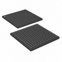
DS26518GN+ Maxim Integrated Products, DS26518GN+ Datasheet - Page 95

DS26518GN+
Manufacturer Part Number
DS26518GN+
Description
IC TXRX T1/E1/J1 8PORT 256-CSBGA
Manufacturer
Maxim Integrated Products
Type
Transceiverr
Specifications of DS26518GN+
Number Of Drivers/receivers
8/8
Protocol
T1/E1/J1
Voltage - Supply
3.135 V ~ 3.465 V
Mounting Type
Surface Mount
Package / Case
256-CSBGA
Lead Free Status / RoHS Status
Lead free / RoHS Compliant
- Current page: 95 of 312
- Download datasheet (3Mb)
9.12.4 Hitless Protection Switching (HPS)
Many current redundancy protection implementations use mechanical relays to switch between primary and
backup boards. The switching time in relays is typically in the milliseconds, making T1/E1 HPS impossible. The
switching event will likely cause frame-synchronization loss in any equipment downstream, affecting the quality of
service. The same is also true for tri-stating mechanisms that use software or inactive clocks for the triggering of
HPS.
The DS26518 LIUs feature fast tristatable outputs for TTIPn and TRINGn and fast disabling of internal impedance
matching for RTIPn and RRINGn within one-bit period. The TXENABLE pin is used for hitless protection circuits in
combination with the LTRCR.RHPM bit. When low, the TXENABLE pin tri-states all eight transmitters, providing a
high-impedance state on TTIPn and TRINGn. If the RHPM bit is set, the TXENABLE pin, when low, will also
disable the internal termination on RTIPn and RRINGn on a per-port basis, providing a high impedance to the
receive line.
This is a very useful function in that control can be done through a hardware pin, allowing a quick switch to the
backup system for both the receiver and the transmitter.
Figure 9-26. HPS Block Diagram
SWITCHING
CONTROL
TXENABLE
TXENABLE
PRIMARY
BACKUP
BOARD
BOARD
95 of 312
RRING
RRING
RTIP
TRING
RTIP
TRING
TTIP
TTIP
Figure 9-26
shows a typical HPS application.
INTERFACE
CARD
LINE
RX
TX
Related parts for DS26518GN+
Image
Part Number
Description
Manufacturer
Datasheet
Request
R

Part Number:
Description:
8-port T1/e1/j1 Transceiver
Manufacturer:
Maxim Integrated Products, Inc.
Datasheet:

Part Number:
Description:
Ds26518 8-port T1/e1/j1 Transceiver
Manufacturer:
Maxim Integrated Products, Inc.

Part Number:
Description:
power light source LUXEON� Collimator
Manufacturer:
LUMILEDS [Lumileds Lighting Company]
Datasheet:

Part Number:
Description:
MAX7528KCWPMaxim Integrated Products [CMOS Dual 8-Bit Buffered Multiplying DACs]
Manufacturer:
Maxim Integrated Products
Datasheet:

Part Number:
Description:
Single +5V, fully integrated, 1.25Gbps laser diode driver.
Manufacturer:
Maxim Integrated Products
Datasheet:

Part Number:
Description:
Single +5V, fully integrated, 155Mbps laser diode driver.
Manufacturer:
Maxim Integrated Products
Datasheet:

Part Number:
Description:
VRD11/VRD10, K8 Rev F 2/3/4-Phase PWM Controllers with Integrated Dual MOSFET Drivers
Manufacturer:
Maxim Integrated Products
Datasheet:

Part Number:
Description:
Highly Integrated Level 2 SMBus Battery Chargers
Manufacturer:
Maxim Integrated Products
Datasheet:

Part Number:
Description:
Current Monitor and Accumulator with Integrated Sense Resistor; ; Temperature Range: -40°C to +85°C
Manufacturer:
Maxim Integrated Products

Part Number:
Description:
TSSOP 14/A�/RS-485 Transceivers with Integrated 100O/120O Termination Resis
Manufacturer:
Maxim Integrated Products

Part Number:
Description:
TSSOP 14/A�/RS-485 Transceivers with Integrated 100O/120O Termination Resis
Manufacturer:
Maxim Integrated Products

Part Number:
Description:
QFN 16/A�/AC-DC and DC-DC Peak-Current-Mode Converters with Integrated Step
Manufacturer:
Maxim Integrated Products

Part Number:
Description:
TDFN/A/65V, 1A, 600KHZ, SYNCHRONOUS STEP-DOWN REGULATOR WITH INTEGRATED SWI
Manufacturer:
Maxim Integrated Products

Part Number:
Description:
Integrated Temperature Controller f
Manufacturer:
Maxim Integrated Products


