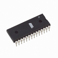
ATTINY48-PU Atmel, ATTINY48-PU Datasheet - Page 101

ATTINY48-PU
Manufacturer Part Number
ATTINY48-PU
Description
MCU AVR 4K ISP FLASH 1.8V 28-DIP
Manufacturer
Atmel
Series
AVR® ATtinyr
Specifications of ATTINY48-PU
Core Processor
AVR
Core Size
8-Bit
Speed
12MHz
Connectivity
I²C, SPI
Peripherals
Brown-out Detect/Reset, POR, WDT
Number Of I /o
24
Program Memory Size
4KB (2K x 16)
Program Memory Type
FLASH
Eeprom Size
64 x 8
Ram Size
256 x 8
Voltage - Supply (vcc/vdd)
1.8 V ~ 5.5 V
Data Converters
A/D 6x10b
Oscillator Type
Internal
Operating Temperature
-40°C ~ 85°C
Package / Case
28-DIP (0.300", 7.62mm)
Processor Series
ATTINY4x
Core
AVR8
Data Bus Width
8 bit
Data Ram Size
256 B
Interface Type
2-Wire/I2S/SPI
Maximum Clock Frequency
12 MHz
Number Of Programmable I/os
28
Number Of Timers
2
Maximum Operating Temperature
+ 85 C
Mounting Style
Through Hole
3rd Party Development Tools
EWAVR, EWAVR-BL
Development Tools By Supplier
ATAVRDRAGON, ATSTK500, ATSTK600, ATAVRISP2, ATAVRONEKIT
Minimum Operating Temperature
- 40 C
On-chip Adc
6-ch x 10-bit
Package
28PDIP
Device Core
AVR
Family Name
ATtiny
Maximum Speed
12 MHz
Operating Supply Voltage
2.5|3.3|5 V
For Use With
ATSTK600 - DEV KIT FOR AVR/AVR32ATAVRDRAGON - KIT DRAGON 32KB FLASH MEM AVRATAVRISP2 - PROGRAMMER AVR IN SYSTEM
Lead Free Status / RoHS Status
Lead free / RoHS Compliant
Available stocks
Company
Part Number
Manufacturer
Quantity
Price
Company:
Part Number:
ATTINY48-PU
Manufacturer:
ATMEL
Quantity:
5 530
Company:
Part Number:
ATTINY48-PU
Manufacturer:
AVX
Quantity:
30 000
- Current page: 101 of 302
- Download datasheet (9Mb)
12.9.3
8008G–AVR–04/11
Fast PWM Mode
The timing diagram for the CTC mode is shown in
increases until a compare match occurs with either OCR1A or ICR1, and then counter (TCNT1)
is cleared.
Figure 12-6. CTC Mode, Timing Diagram
An interrupt can be generated at each time the counter value reaches the TOP value by either
using the OCF1A or ICF1 Flag according to the register used to define the TOP value. If the
interrupt is enabled, the interrupt handler routine can be used for updating the TOP value. How-
ever, changing the TOP to a value close to BOTTOM when the counter is running with none or a
low prescaler value must be done with care since the CTC mode does not have the double buff-
ering feature. If the new value written to OCR1A or ICR1 is lower than the current value of
TCNT1, the counter will miss the compare match. The counter will then have to count to its max-
imum value (0xFFFF) and wrap around starting at 0x0000 before the compare match can occur.
In many cases this feature is not desirable. An alternative will then be to use the fast PWM mode
using OCR1A for defining TOP (WGM1[3:0] = 15) since the OCR1A then will be double buffered.
For generating a waveform output in CTC mode, the OC1A output can be set to toggle its logical
level on each compare match by setting the Compare Output mode bits to toggle mode
(COM1A[1:0] = 1). The OC1A value will not be visible on the port pin unless the data direction
for the pin is set to output (DDR_OC1A = 1). The waveform generated will have a maximum fre-
quency of f
defined by the following equation:
The N variable represents the prescaler factor (1, 8, 64, 256, or 1024).
As for the Normal mode of operation, the TOV1 Flag is set in the same timer clock cycle that the
counter counts from MAX to 0x0000.
The fast Pulse Width Modulation or fast PWM mode (WGM1[3:0] = 5, 6, 7, 14, or 15) provides a
high frequency PWM waveform generation option. The fast PWM differs from the other PWM
options by its single-slope operation. The counter counts from BOTTOM to TOP then restarts
from BOTTOM. In non-inverting Compare Output mode, the Output Compare (OC1x) is set on
the compare match between TCNT1 and OCR1x, and cleared at TOP. In inverting Compare
Output mode output is cleared on compare match and set at TOP. Due to the single-slope oper-
TCNTn
OCnA
(Toggle)
Period
OC
1
A
= f
1
clk_I/O
/2 when OCR1A is set to zero (0x0000). The waveform frequency is
f
OCnA
2
=
-------------------------------------------------- -
2 N
3
⋅
⋅
(
f
1
clk_I/O
+
Figure
OCRnA
4
12-6. The counter value (TCNT1)
)
ATtiny48/88
OCnA Interrupt Flag Set
or ICFn Interrupt Flag Set
(Interrupt on TOP)
(COMnA[1:0] = 1)
101
Related parts for ATTINY48-PU
Image
Part Number
Description
Manufacturer
Datasheet
Request
R

Part Number:
Description:
Manufacturer:
Atmel Corporation
Datasheet:

Part Number:
Description:
Microcontrollers (MCU) 512B FL 32B SRAM TIMER ATTINY4 12MHz
Manufacturer:
Atmel

Part Number:
Description:
IC MCU AVR 512B FLASH SOT-23-6
Manufacturer:
Atmel
Datasheet:

Part Number:
Description:
IC MCU AVR 512B FLASH SOT-23-6
Manufacturer:
Atmel
Datasheet:

Part Number:
Description:
IC, MCU, 8BIT, 2K FLASH, 20SOIC
Manufacturer:
Atmel
Datasheet:

Part Number:
Description:
IC, MCU, 8BIT, 2K FLASH, 20PDIP
Manufacturer:
Atmel
Datasheet:

Part Number:
Description:
IC, MCU, 8BIT, 8K FLASH, 20PDIP
Manufacturer:
Atmel
Datasheet:

Part Number:
Description:
IC, MCU, 8BIT, 8K FLASH, 20SOIC
Manufacturer:
Atmel
Datasheet:

Part Number:
Description:
DEV KIT FOR AVR/AVR32
Manufacturer:
Atmel
Datasheet:

Part Number:
Description:
INTERVAL AND WIPE/WASH WIPER CONTROL IC WITH DELAY
Manufacturer:
ATMEL Corporation
Datasheet:

Part Number:
Description:
Low-Voltage Voice-Switched IC for Hands-Free Operation
Manufacturer:
ATMEL Corporation
Datasheet:

Part Number:
Description:
MONOLITHIC INTEGRATED FEATUREPHONE CIRCUIT
Manufacturer:
ATMEL Corporation
Datasheet:

Part Number:
Description:
AM-FM Receiver IC U4255BM-M
Manufacturer:
ATMEL Corporation
Datasheet:


