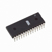
ATTINY48-PU Atmel, ATTINY48-PU Datasheet - Page 185

ATTINY48-PU
Manufacturer Part Number
ATTINY48-PU
Description
MCU AVR 4K ISP FLASH 1.8V 28-DIP
Manufacturer
Atmel
Series
AVR® ATtinyr
Specifications of ATTINY48-PU
Core Processor
AVR
Core Size
8-Bit
Speed
12MHz
Connectivity
I²C, SPI
Peripherals
Brown-out Detect/Reset, POR, WDT
Number Of I /o
24
Program Memory Size
4KB (2K x 16)
Program Memory Type
FLASH
Eeprom Size
64 x 8
Ram Size
256 x 8
Voltage - Supply (vcc/vdd)
1.8 V ~ 5.5 V
Data Converters
A/D 6x10b
Oscillator Type
Internal
Operating Temperature
-40°C ~ 85°C
Package / Case
28-DIP (0.300", 7.62mm)
Processor Series
ATTINY4x
Core
AVR8
Data Bus Width
8 bit
Data Ram Size
256 B
Interface Type
2-Wire/I2S/SPI
Maximum Clock Frequency
12 MHz
Number Of Programmable I/os
28
Number Of Timers
2
Maximum Operating Temperature
+ 85 C
Mounting Style
Through Hole
3rd Party Development Tools
EWAVR, EWAVR-BL
Development Tools By Supplier
ATAVRDRAGON, ATSTK500, ATSTK600, ATAVRISP2, ATAVRONEKIT
Minimum Operating Temperature
- 40 C
On-chip Adc
6-ch x 10-bit
Package
28PDIP
Device Core
AVR
Family Name
ATtiny
Maximum Speed
12 MHz
Operating Supply Voltage
2.5|3.3|5 V
For Use With
ATSTK600 - DEV KIT FOR AVR/AVR32ATAVRDRAGON - KIT DRAGON 32KB FLASH MEM AVRATAVRISP2 - PROGRAMMER AVR IN SYSTEM
Lead Free Status / RoHS Status
Lead free / RoHS Compliant
Available stocks
Company
Part Number
Manufacturer
Quantity
Price
Company:
Part Number:
ATTINY48-PU
Manufacturer:
ATMEL
Quantity:
5 530
Company:
Part Number:
ATTINY48-PU
Manufacturer:
AVX
Quantity:
30 000
- Current page: 185 of 302
- Download datasheet (9Mb)
19.1.1
19.1.2
8008G–AVR–04/11
EEPROM Write Prevents Writing to SPMCSR
Reading the Fuse and Lock Bits from Software
Note that an EEPROM write operation will block all software programming to Flash. Reading the
Fuses and Lock bits from software will also be prevented during the EEPROM write operation. It
is recommended that the user checks the status bit (EEPE) in the EECR Register and verifies
that the bit is cleared before writing to the SPMCSR Register.
It is possible to read both the Fuse and Lock bits from software. To read the Lock bits, load the
Z-pointer with 0x0001 and set the RFLB and SELFPRGEN bits in SPMCSR. When an LPM
instruction is executed within three CPU cycles after the RFLB and SELFPRGEN bits are set in
SPMCSR, the value of the Lock bits will be loaded in the destination register. The RFLB and
SELFPRGEN bits will auto-clear upon completion of reading the Lock bits or if no LPM instruc-
tion is executed within three CPU cycles or no SPM instruction is executed within four CPU
cycles. When RFLB and SELFPRGEN are cleared, LPM will work as described in the Instruction
set Manual.
The algorithm for reading the Fuse Low byte is similar to the one described above for reading
the Lock bits. To read the Fuse Low byte, load the Z-pointer with 0x0000 and set the RFLB and
SELFPRGEN bits in SPMCSR. When an LPM instruction is executed within three cycles after
the RFLB and SELFPRGEN bits are set in the SPMCSR, the value of the Fuse Low byte (FLB)
will be loaded in the destination register as shown below.See
detailed description and mapping of the Fuse Low byte.
Similarly, when reading the Fuse High byte (FHB), load 0x0003 in the Z-pointer. When an LPM
instruction is executed within three cycles after the RFLB and SELFPRGEN bits are set in the
SPMCSR, the value of the Fuse High byte will be loaded in the destination register as shown
below. See
Fuse Extended byte can be read by loading the Z-pointer with 0x0002. When an LPM instruction
is executed within three cycles after the RFLB and SPMEN bits are set in the SPMCSR, the
value of the Fuse Extended Byte (FEB) will be loaded in the destination register as shown
below. See
byte.
Fuse and Lock bits that are programmed, will be read as zero. Fuse and Lock bits that are
unprogrammed, will be read as one.
Bit
Rd
Bit
Rd
Bit
Rd
Bit
Rd
Table 20-4 on page 189
Table 20-3 on page 189
FHB7
FLB7
FEB7
7
7
7
7
–
FHB6
FLB6
FEB6
6
6
6
6
–
FHB5
FEB5
FLB5
5
5
5
5
–
for detailed description and mapping of the Fuse High byte.
for detailed description and mapping of the Fuse Extended
FHB4
FEB4
FLB4
4
–
4
4
4
FHB3
FLB3
FEB3
3
–
3
3
3
FHB2
FEB2
FLB2
2
–
2
2
2
Table 20-5 on page 190
FHB1
FLB1
FEB1
LB2
1
1
1
1
ATtiny48/88
FHB0
FLB0
FEB0
LB1
0
0
0
0
for a
185
Related parts for ATTINY48-PU
Image
Part Number
Description
Manufacturer
Datasheet
Request
R

Part Number:
Description:
Manufacturer:
Atmel Corporation
Datasheet:

Part Number:
Description:
Microcontrollers (MCU) 512B FL 32B SRAM TIMER ATTINY4 12MHz
Manufacturer:
Atmel

Part Number:
Description:
IC MCU AVR 512B FLASH SOT-23-6
Manufacturer:
Atmel
Datasheet:

Part Number:
Description:
IC MCU AVR 512B FLASH SOT-23-6
Manufacturer:
Atmel
Datasheet:

Part Number:
Description:
IC, MCU, 8BIT, 2K FLASH, 20SOIC
Manufacturer:
Atmel
Datasheet:

Part Number:
Description:
IC, MCU, 8BIT, 2K FLASH, 20PDIP
Manufacturer:
Atmel
Datasheet:

Part Number:
Description:
IC, MCU, 8BIT, 8K FLASH, 20PDIP
Manufacturer:
Atmel
Datasheet:

Part Number:
Description:
IC, MCU, 8BIT, 8K FLASH, 20SOIC
Manufacturer:
Atmel
Datasheet:

Part Number:
Description:
DEV KIT FOR AVR/AVR32
Manufacturer:
Atmel
Datasheet:

Part Number:
Description:
INTERVAL AND WIPE/WASH WIPER CONTROL IC WITH DELAY
Manufacturer:
ATMEL Corporation
Datasheet:

Part Number:
Description:
Low-Voltage Voice-Switched IC for Hands-Free Operation
Manufacturer:
ATMEL Corporation
Datasheet:

Part Number:
Description:
MONOLITHIC INTEGRATED FEATUREPHONE CIRCUIT
Manufacturer:
ATMEL Corporation
Datasheet:

Part Number:
Description:
AM-FM Receiver IC U4255BM-M
Manufacturer:
ATMEL Corporation
Datasheet:


