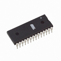
ATTINY48-PU Atmel, ATTINY48-PU Datasheet - Page 132

ATTINY48-PU
Manufacturer Part Number
ATTINY48-PU
Description
MCU AVR 4K ISP FLASH 1.8V 28-DIP
Manufacturer
Atmel
Series
AVR® ATtinyr
Specifications of ATTINY48-PU
Core Processor
AVR
Core Size
8-Bit
Speed
12MHz
Connectivity
I²C, SPI
Peripherals
Brown-out Detect/Reset, POR, WDT
Number Of I /o
24
Program Memory Size
4KB (2K x 16)
Program Memory Type
FLASH
Eeprom Size
64 x 8
Ram Size
256 x 8
Voltage - Supply (vcc/vdd)
1.8 V ~ 5.5 V
Data Converters
A/D 6x10b
Oscillator Type
Internal
Operating Temperature
-40°C ~ 85°C
Package / Case
28-DIP (0.300", 7.62mm)
Processor Series
ATTINY4x
Core
AVR8
Data Bus Width
8 bit
Data Ram Size
256 B
Interface Type
2-Wire/I2S/SPI
Maximum Clock Frequency
12 MHz
Number Of Programmable I/os
28
Number Of Timers
2
Maximum Operating Temperature
+ 85 C
Mounting Style
Through Hole
3rd Party Development Tools
EWAVR, EWAVR-BL
Development Tools By Supplier
ATAVRDRAGON, ATSTK500, ATSTK600, ATAVRISP2, ATAVRONEKIT
Minimum Operating Temperature
- 40 C
On-chip Adc
6-ch x 10-bit
Package
28PDIP
Device Core
AVR
Family Name
ATtiny
Maximum Speed
12 MHz
Operating Supply Voltage
2.5|3.3|5 V
For Use With
ATSTK600 - DEV KIT FOR AVR/AVR32ATAVRDRAGON - KIT DRAGON 32KB FLASH MEM AVRATAVRISP2 - PROGRAMMER AVR IN SYSTEM
Lead Free Status / RoHS Status
Lead free / RoHS Compliant
Available stocks
Company
Part Number
Manufacturer
Quantity
Price
Company:
Part Number:
ATTINY48-PU
Manufacturer:
ATMEL
Quantity:
5 530
Company:
Part Number:
ATTINY48-PU
Manufacturer:
AVX
Quantity:
30 000
- Current page: 132 of 302
- Download datasheet (9Mb)
15.4.4
15.4.5
132
ATtiny48/88
Data Packet Format
Combining Address and Data Packets into a Transmission
The MSB of the address byte is transmitted first. Slave addresses can freely be allocated by the
designer, but the address 0000 000 is reserved for a general call.
When a general call is issued, all slaves should respond by pulling the SDA line low in the ACK
cycle. A general call is used when a Master wishes to transmit the same message to several
slaves in the system. When the general call address followed by a Write bit is transmitted on the
bus, all slaves set up to acknowledge the general call will pull the SDA line low in the ack cycle.
The following data packets will then be received by all the slaves that acknowledged the general
call. Note that transmitting the general call address followed by a Read bit is meaningless, as
this would cause contention if several slaves started transmitting different data.
All addresses of the format 1111 xxx should be reserved for future purposes.
All data packets transmitted on the TWI bus are nine bits long, consisting of one data byte and
an acknowledge bit. During a data transfer, the Master generates the clock and the START and
STOP conditions, while the Receiver is responsible for acknowledging the reception. An
Acknowledge (ACK) is signalled by the Receiver pulling the SDA line low during the ninth SCL
cycle. If the Receiver leaves the SDA line high, a NACK is signalled. When the Receiver has
received the last byte, or for some reason cannot receive any more bytes, it should inform the
Transmitter by sending a NACK after the final byte. The MSB of the data byte is transmitted first.
Figure 15-5. Data Packet Format
A transmission basically consists of a START condition, a SLA+R/W, one or more data packets
and a STOP condition. An empty message, consisting of a START followed by a STOP condi-
tion, is illegal. Note that the Wired-ANDing of the SCL line can be used to implement
handshaking between the Master and the Slave. The Slave can extend the SCL low period by
pulling the SCL line low. This is useful if the clock speed set up by the Master is too fast for the
Slave, or the Slave needs extra time for processing between the data transmissions. The Slave
extending the SCL low period will not affect the SCL high period, which is determined by the
Master. As a consequence, the Slave can reduce the TWI data transfer speed by prolonging the
SCL duty cycle.
Figure 15-6
between the SLA+R/W and the STOP condition, depending on the software protocol imple-
mented by the application software.
Transmitter
Aggregate
SDA from
SDA from
SCL from
Receiver
Master
SDA
SLA+R/W
shows a typical data transmission. Note that several data bytes can be transmitted
Data MSB
1
2
Data Byte
7
Data LSB
8
ACK
9
STOP, REPEATED
START or Next
8008G–AVR–04/11
Data Byte
Related parts for ATTINY48-PU
Image
Part Number
Description
Manufacturer
Datasheet
Request
R

Part Number:
Description:
Manufacturer:
Atmel Corporation
Datasheet:

Part Number:
Description:
Microcontrollers (MCU) 512B FL 32B SRAM TIMER ATTINY4 12MHz
Manufacturer:
Atmel

Part Number:
Description:
IC MCU AVR 512B FLASH SOT-23-6
Manufacturer:
Atmel
Datasheet:

Part Number:
Description:
IC MCU AVR 512B FLASH SOT-23-6
Manufacturer:
Atmel
Datasheet:

Part Number:
Description:
IC, MCU, 8BIT, 2K FLASH, 20SOIC
Manufacturer:
Atmel
Datasheet:

Part Number:
Description:
IC, MCU, 8BIT, 2K FLASH, 20PDIP
Manufacturer:
Atmel
Datasheet:

Part Number:
Description:
IC, MCU, 8BIT, 8K FLASH, 20PDIP
Manufacturer:
Atmel
Datasheet:

Part Number:
Description:
IC, MCU, 8BIT, 8K FLASH, 20SOIC
Manufacturer:
Atmel
Datasheet:

Part Number:
Description:
DEV KIT FOR AVR/AVR32
Manufacturer:
Atmel
Datasheet:

Part Number:
Description:
INTERVAL AND WIPE/WASH WIPER CONTROL IC WITH DELAY
Manufacturer:
ATMEL Corporation
Datasheet:

Part Number:
Description:
Low-Voltage Voice-Switched IC for Hands-Free Operation
Manufacturer:
ATMEL Corporation
Datasheet:

Part Number:
Description:
MONOLITHIC INTEGRATED FEATUREPHONE CIRCUIT
Manufacturer:
ATMEL Corporation
Datasheet:

Part Number:
Description:
AM-FM Receiver IC U4255BM-M
Manufacturer:
ATMEL Corporation
Datasheet:


