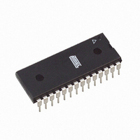
ATTINY48-PU Atmel, ATTINY48-PU Datasheet - Page 72

ATTINY48-PU
Manufacturer Part Number
ATTINY48-PU
Description
MCU AVR 4K ISP FLASH 1.8V 28-DIP
Manufacturer
Atmel
Series
AVR® ATtinyr
Specifications of ATTINY48-PU
Core Processor
AVR
Core Size
8-Bit
Speed
12MHz
Connectivity
I²C, SPI
Peripherals
Brown-out Detect/Reset, POR, WDT
Number Of I /o
24
Program Memory Size
4KB (2K x 16)
Program Memory Type
FLASH
Eeprom Size
64 x 8
Ram Size
256 x 8
Voltage - Supply (vcc/vdd)
1.8 V ~ 5.5 V
Data Converters
A/D 6x10b
Oscillator Type
Internal
Operating Temperature
-40°C ~ 85°C
Package / Case
28-DIP (0.300", 7.62mm)
Processor Series
ATTINY4x
Core
AVR8
Data Bus Width
8 bit
Data Ram Size
256 B
Interface Type
2-Wire/I2S/SPI
Maximum Clock Frequency
12 MHz
Number Of Programmable I/os
28
Number Of Timers
2
Maximum Operating Temperature
+ 85 C
Mounting Style
Through Hole
3rd Party Development Tools
EWAVR, EWAVR-BL
Development Tools By Supplier
ATAVRDRAGON, ATSTK500, ATSTK600, ATAVRISP2, ATAVRONEKIT
Minimum Operating Temperature
- 40 C
On-chip Adc
6-ch x 10-bit
Package
28PDIP
Device Core
AVR
Family Name
ATtiny
Maximum Speed
12 MHz
Operating Supply Voltage
2.5|3.3|5 V
For Use With
ATSTK600 - DEV KIT FOR AVR/AVR32ATAVRDRAGON - KIT DRAGON 32KB FLASH MEM AVRATAVRISP2 - PROGRAMMER AVR IN SYSTEM
Lead Free Status / RoHS Status
Lead free / RoHS Compliant
Available stocks
Company
Part Number
Manufacturer
Quantity
Price
Company:
Part Number:
ATTINY48-PU
Manufacturer:
ATMEL
Quantity:
5 530
Company:
Part Number:
ATTINY48-PU
Manufacturer:
AVX
Quantity:
30 000
- Current page: 72 of 302
- Download datasheet (9Mb)
10.3.3
72
ATtiny48/88
Alternate Functions of Port C
The Port C pins with alternate functions are shown in
Table 10-8.
The alternate pin configuration is as follows:
• PCINT15 – Port C, Bit 7
PCINT15: Pin Change Interrupt source 15. The PC7 pin can serve as an external interrupt
source.
• RESET/PCINT14 – Port C, Bit 6
RESET, Reset pin: When the RSTDISBL Fuse is programmed, this pin functions as a normal I/O
pin, and the part will have to rely on Power-on Reset and Brown-out Reset as its reset sources.
When the RSTDISBL Fuse is unprogrammed, the reset circuitry is connected to the pin, and the
pin can not be used as an I/O pin.
If PC6 is used as a reset pin, DDC6, PORTC6 and PINC6 will all read 0.
PCINT14: Pin Change Interrupt source 14. The PC6 pin can serve as an external interrupt
source.
• SCL/ADC5/PCINT13 – Port C, Bit 5
SCL, 2-wire Serial Interface Clock: When the TWEN bit in TWCR is set (one) to enable the 2-
wire Serial Interface, pin PC5 is disconnected from the port and becomes the Serial Clock I/O
pin for the 2-wire Serial Interface. In this mode, there is a spike filter on the pin to suppress
spikes shorter than 50 ns on the input signal, and the pin is driven by an open drain driver with
slew-rate limitation.
PC5 can also be used as ADC input Channel 5. Note that ADC input channel 5 uses digital
power.
Port Pin
PC7
PC6
PC5
PC4
PC3
PC2
PC1
PC0
Port C Pins Alternate Functions
Alternate Function
PCINT15 (Pin Change Interrupt 15)
RESET (Reset pin)
PCINT14 (Pin Change Interrupt 14)
ADC5 (ADC Input Channel 5)
SCL (2-wire Serial Bus Clock Line)
PCINT13 (Pin Change Interrupt 13)
ADC4 (ADC Input Channel 4)
SDA (2-wire Serial Bus Data Input/Output Line)
PCINT12 (Pin Change Interrupt 12)
ADC3 (ADC Input Channel 3)
PCINT11 (Pin Change Interrupt 11)
ADC2 (ADC Input Channel 2)
PCINT10 (Pin Change Interrupt 10)
ADC1 (ADC Input Channel 1)
PCINT9 (Pin Change Interrupt 9)
ADC0 (ADC Input Channel 0)
PCINT8 (Pin Change Interrupt 8)
Table
10-8.
8008G–AVR–04/11
Related parts for ATTINY48-PU
Image
Part Number
Description
Manufacturer
Datasheet
Request
R

Part Number:
Description:
Manufacturer:
Atmel Corporation
Datasheet:

Part Number:
Description:
Microcontrollers (MCU) 512B FL 32B SRAM TIMER ATTINY4 12MHz
Manufacturer:
Atmel

Part Number:
Description:
IC MCU AVR 512B FLASH SOT-23-6
Manufacturer:
Atmel
Datasheet:

Part Number:
Description:
IC MCU AVR 512B FLASH SOT-23-6
Manufacturer:
Atmel
Datasheet:

Part Number:
Description:
IC, MCU, 8BIT, 2K FLASH, 20SOIC
Manufacturer:
Atmel
Datasheet:

Part Number:
Description:
IC, MCU, 8BIT, 2K FLASH, 20PDIP
Manufacturer:
Atmel
Datasheet:

Part Number:
Description:
IC, MCU, 8BIT, 8K FLASH, 20PDIP
Manufacturer:
Atmel
Datasheet:

Part Number:
Description:
IC, MCU, 8BIT, 8K FLASH, 20SOIC
Manufacturer:
Atmel
Datasheet:

Part Number:
Description:
DEV KIT FOR AVR/AVR32
Manufacturer:
Atmel
Datasheet:

Part Number:
Description:
INTERVAL AND WIPE/WASH WIPER CONTROL IC WITH DELAY
Manufacturer:
ATMEL Corporation
Datasheet:

Part Number:
Description:
Low-Voltage Voice-Switched IC for Hands-Free Operation
Manufacturer:
ATMEL Corporation
Datasheet:

Part Number:
Description:
MONOLITHIC INTEGRATED FEATUREPHONE CIRCUIT
Manufacturer:
ATMEL Corporation
Datasheet:

Part Number:
Description:
AM-FM Receiver IC U4255BM-M
Manufacturer:
ATMEL Corporation
Datasheet:


