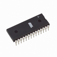
ATTINY48-PU Atmel, ATTINY48-PU Datasheet - Page 193

ATTINY48-PU
Manufacturer Part Number
ATTINY48-PU
Description
MCU AVR 4K ISP FLASH 1.8V 28-DIP
Manufacturer
Atmel
Series
AVR® ATtinyr
Specifications of ATTINY48-PU
Core Processor
AVR
Core Size
8-Bit
Speed
12MHz
Connectivity
I²C, SPI
Peripherals
Brown-out Detect/Reset, POR, WDT
Number Of I /o
24
Program Memory Size
4KB (2K x 16)
Program Memory Type
FLASH
Eeprom Size
64 x 8
Ram Size
256 x 8
Voltage - Supply (vcc/vdd)
1.8 V ~ 5.5 V
Data Converters
A/D 6x10b
Oscillator Type
Internal
Operating Temperature
-40°C ~ 85°C
Package / Case
28-DIP (0.300", 7.62mm)
Processor Series
ATTINY4x
Core
AVR8
Data Bus Width
8 bit
Data Ram Size
256 B
Interface Type
2-Wire/I2S/SPI
Maximum Clock Frequency
12 MHz
Number Of Programmable I/os
28
Number Of Timers
2
Maximum Operating Temperature
+ 85 C
Mounting Style
Through Hole
3rd Party Development Tools
EWAVR, EWAVR-BL
Development Tools By Supplier
ATAVRDRAGON, ATSTK500, ATSTK600, ATAVRISP2, ATAVRONEKIT
Minimum Operating Temperature
- 40 C
On-chip Adc
6-ch x 10-bit
Package
28PDIP
Device Core
AVR
Family Name
ATtiny
Maximum Speed
12 MHz
Operating Supply Voltage
2.5|3.3|5 V
For Use With
ATSTK600 - DEV KIT FOR AVR/AVR32ATAVRDRAGON - KIT DRAGON 32KB FLASH MEM AVRATAVRISP2 - PROGRAMMER AVR IN SYSTEM
Lead Free Status / RoHS Status
Lead free / RoHS Compliant
Available stocks
Company
Part Number
Manufacturer
Quantity
Price
Company:
Part Number:
ATTINY48-PU
Manufacturer:
ATMEL
Quantity:
5 530
Company:
Part Number:
ATTINY48-PU
Manufacturer:
AVX
Quantity:
30 000
- Current page: 193 of 302
- Download datasheet (9Mb)
21.2.1
21.2.2
8008G–AVR–04/11
Enter Programming Mode
Considerations for Efficient Programming
When pulsing WR or OE, the command loaded determines the action executed. The different
Commands are shown in
Table 21-6.
The following algorithm puts the device in Parallel (High-voltage) Programming mode:
If the rise time of the V
tive algorithm can be used.
The loaded command and address are retained in the device during programming. For efficient
programming, the following should be considered.
1. Set Prog_enable pins listed in
2. Apply 4.5 – 5.5V between V
3. Wait 20 – 60 µs, and apply 11.5 – 12.5V to RESET.
4. Keep the Prog_enable pins unchanged for at least 10µs after the High-voltage has
5. Wait at least 300 µs before giving any parallel programming commands.
6. Exit Programming mode by power the device down or by bringing RESET pin to 0V.
1. Set Prog_enable pins listed in
2. Apply 4.5 – 5.5V between V
3. Monitor V
4. Keep the Prog_enable pins unchanged for at least 10µs after the High-voltage has
5. Wait until V
6. Exit Programming mode by power the device down or by bringing RESET pin to 0V.
Command Byte
1000 0000
0100 0000
0010 0000
0001 0000
0001 0001
0000 1000
0000 0100
0000 0010
0000 0011
V
the next 20 µs.
been applied to ensure the Prog_enable Signature has been latched.
V
been applied to ensure the Prog_enable Signature has been latched.
commands.
CC
CC
to 0V.
to 0V.
Command Byte Bit Coding
CC
CC
, and as soon as V
actually reaches 4.5 -5.5V before giving any parallel programming
Command Executed
Chip Erase
Write Fuse bits
Write Lock bits
Write Flash
Write EEPROM
Read Signature Bytes and Calibration byte
Read Fuse and Lock bits
Read Flash
Read EEPROM
CC
Table
is unable to fulfill the requirements listed above, the following alterna-
21-6.
CC
CC
Table 21-4 on page 192
Table 21-4 on page 192
CC
and GND. Ensure that V
and GND.
reaches 0.9 – 1.1V, apply 11.5 – 12.5V to RESET.
to “0000”, RESET pin to 0V and
to “0000”, RESET pin to 0V and
CC
reaches at least 1.8V within
ATtiny48/88
193
Related parts for ATTINY48-PU
Image
Part Number
Description
Manufacturer
Datasheet
Request
R

Part Number:
Description:
Manufacturer:
Atmel Corporation
Datasheet:

Part Number:
Description:
Microcontrollers (MCU) 512B FL 32B SRAM TIMER ATTINY4 12MHz
Manufacturer:
Atmel

Part Number:
Description:
IC MCU AVR 512B FLASH SOT-23-6
Manufacturer:
Atmel
Datasheet:

Part Number:
Description:
IC MCU AVR 512B FLASH SOT-23-6
Manufacturer:
Atmel
Datasheet:

Part Number:
Description:
IC, MCU, 8BIT, 2K FLASH, 20SOIC
Manufacturer:
Atmel
Datasheet:

Part Number:
Description:
IC, MCU, 8BIT, 2K FLASH, 20PDIP
Manufacturer:
Atmel
Datasheet:

Part Number:
Description:
IC, MCU, 8BIT, 8K FLASH, 20PDIP
Manufacturer:
Atmel
Datasheet:

Part Number:
Description:
IC, MCU, 8BIT, 8K FLASH, 20SOIC
Manufacturer:
Atmel
Datasheet:

Part Number:
Description:
DEV KIT FOR AVR/AVR32
Manufacturer:
Atmel
Datasheet:

Part Number:
Description:
INTERVAL AND WIPE/WASH WIPER CONTROL IC WITH DELAY
Manufacturer:
ATMEL Corporation
Datasheet:

Part Number:
Description:
Low-Voltage Voice-Switched IC for Hands-Free Operation
Manufacturer:
ATMEL Corporation
Datasheet:

Part Number:
Description:
MONOLITHIC INTEGRATED FEATUREPHONE CIRCUIT
Manufacturer:
ATMEL Corporation
Datasheet:

Part Number:
Description:
AM-FM Receiver IC U4255BM-M
Manufacturer:
ATMEL Corporation
Datasheet:


