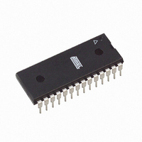
ATTINY48-PU Atmel, ATTINY48-PU Datasheet - Page 85

ATTINY48-PU
Manufacturer Part Number
ATTINY48-PU
Description
MCU AVR 4K ISP FLASH 1.8V 28-DIP
Manufacturer
Atmel
Series
AVR® ATtinyr
Specifications of ATTINY48-PU
Core Processor
AVR
Core Size
8-Bit
Speed
12MHz
Connectivity
I²C, SPI
Peripherals
Brown-out Detect/Reset, POR, WDT
Number Of I /o
24
Program Memory Size
4KB (2K x 16)
Program Memory Type
FLASH
Eeprom Size
64 x 8
Ram Size
256 x 8
Voltage - Supply (vcc/vdd)
1.8 V ~ 5.5 V
Data Converters
A/D 6x10b
Oscillator Type
Internal
Operating Temperature
-40°C ~ 85°C
Package / Case
28-DIP (0.300", 7.62mm)
Processor Series
ATTINY4x
Core
AVR8
Data Bus Width
8 bit
Data Ram Size
256 B
Interface Type
2-Wire/I2S/SPI
Maximum Clock Frequency
12 MHz
Number Of Programmable I/os
28
Number Of Timers
2
Maximum Operating Temperature
+ 85 C
Mounting Style
Through Hole
3rd Party Development Tools
EWAVR, EWAVR-BL
Development Tools By Supplier
ATAVRDRAGON, ATSTK500, ATSTK600, ATAVRISP2, ATAVRONEKIT
Minimum Operating Temperature
- 40 C
On-chip Adc
6-ch x 10-bit
Package
28PDIP
Device Core
AVR
Family Name
ATtiny
Maximum Speed
12 MHz
Operating Supply Voltage
2.5|3.3|5 V
For Use With
ATSTK600 - DEV KIT FOR AVR/AVR32ATAVRDRAGON - KIT DRAGON 32KB FLASH MEM AVRATAVRISP2 - PROGRAMMER AVR IN SYSTEM
Lead Free Status / RoHS Status
Lead free / RoHS Compliant
Available stocks
Company
Part Number
Manufacturer
Quantity
Price
Company:
Part Number:
ATTINY48-PU
Manufacturer:
ATMEL
Quantity:
5 530
Company:
Part Number:
ATTINY48-PU
Manufacturer:
AVX
Quantity:
30 000
- Current page: 85 of 302
- Download datasheet (9Mb)
11.8
11.8.1
8008G–AVR–04/11
8-bit Timer/Counter Register Description
TCCR0A – Timer/Counter Control Register A
Figure 11-7. Timer/Counter Timing Diagram, Setting of OCF0x, with Prescaler (f
Figure 11-8
is TOP.
Figure 11-8. Timer/Counter Timing Diagram, Clear Timer on Compare Match mode, with Pres-
• Bits 7:4 – Res: Reserved Bits
These bits are reserved and will always read zero.
• Bit 3 – CTC0: Clear Timer on Compare Match Mode
This bit control the counting sequence of the counter, the source for maximum (TOP) counter
value, see
mode (counter), Clear Timer on Compare Match (CTC) mode (see
page
Bit
0x25 (0x45)
Read/Write
Initial Value
TCNTn
TCNTn
(clk
(clk
OCRnx
OCRnx
83).
OCFnx
(CTC)
OCFnx
clk
clk
clk
clk
I/O
I/O
I/O
Tn
I/O
Tn
/8)
/8)
Table
shows the setting of OCF0A and the clearing of TCNT0 in CTC mode where OCR0A
caler (f
7
R
0
–
11-2. Modes of operation supported by the Timer/Counter unit are: Normal
clk_I/O
OCRnx - 1
TOP - 1
/8)
R
6
0
–
R
5
–
0
OCRnx
TOP
R
4
–
0
OCRnx Value
TOP
CTC0
R/W
3
0
OCRnx + 1
BOTTOM
CS02
R/W
2
0
“Modes of Operation” on
CS01
R/W
1
0
ATtiny48/88
BOTTOM + 1
CS00
OCRnx + 2
R/W
0
0
clk_I/O
/8)
TCCR0A
85
Related parts for ATTINY48-PU
Image
Part Number
Description
Manufacturer
Datasheet
Request
R

Part Number:
Description:
Manufacturer:
Atmel Corporation
Datasheet:

Part Number:
Description:
Microcontrollers (MCU) 512B FL 32B SRAM TIMER ATTINY4 12MHz
Manufacturer:
Atmel

Part Number:
Description:
IC MCU AVR 512B FLASH SOT-23-6
Manufacturer:
Atmel
Datasheet:

Part Number:
Description:
IC MCU AVR 512B FLASH SOT-23-6
Manufacturer:
Atmel
Datasheet:

Part Number:
Description:
IC, MCU, 8BIT, 2K FLASH, 20SOIC
Manufacturer:
Atmel
Datasheet:

Part Number:
Description:
IC, MCU, 8BIT, 2K FLASH, 20PDIP
Manufacturer:
Atmel
Datasheet:

Part Number:
Description:
IC, MCU, 8BIT, 8K FLASH, 20PDIP
Manufacturer:
Atmel
Datasheet:

Part Number:
Description:
IC, MCU, 8BIT, 8K FLASH, 20SOIC
Manufacturer:
Atmel
Datasheet:

Part Number:
Description:
DEV KIT FOR AVR/AVR32
Manufacturer:
Atmel
Datasheet:

Part Number:
Description:
INTERVAL AND WIPE/WASH WIPER CONTROL IC WITH DELAY
Manufacturer:
ATMEL Corporation
Datasheet:

Part Number:
Description:
Low-Voltage Voice-Switched IC for Hands-Free Operation
Manufacturer:
ATMEL Corporation
Datasheet:

Part Number:
Description:
MONOLITHIC INTEGRATED FEATUREPHONE CIRCUIT
Manufacturer:
ATMEL Corporation
Datasheet:

Part Number:
Description:
AM-FM Receiver IC U4255BM-M
Manufacturer:
ATMEL Corporation
Datasheet:


