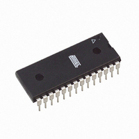
ATTINY48-PU Atmel, ATTINY48-PU Datasheet - Page 111

ATTINY48-PU
Manufacturer Part Number
ATTINY48-PU
Description
MCU AVR 4K ISP FLASH 1.8V 28-DIP
Manufacturer
Atmel
Series
AVR® ATtinyr
Specifications of ATTINY48-PU
Core Processor
AVR
Core Size
8-Bit
Speed
12MHz
Connectivity
I²C, SPI
Peripherals
Brown-out Detect/Reset, POR, WDT
Number Of I /o
24
Program Memory Size
4KB (2K x 16)
Program Memory Type
FLASH
Eeprom Size
64 x 8
Ram Size
256 x 8
Voltage - Supply (vcc/vdd)
1.8 V ~ 5.5 V
Data Converters
A/D 6x10b
Oscillator Type
Internal
Operating Temperature
-40°C ~ 85°C
Package / Case
28-DIP (0.300", 7.62mm)
Processor Series
ATTINY4x
Core
AVR8
Data Bus Width
8 bit
Data Ram Size
256 B
Interface Type
2-Wire/I2S/SPI
Maximum Clock Frequency
12 MHz
Number Of Programmable I/os
28
Number Of Timers
2
Maximum Operating Temperature
+ 85 C
Mounting Style
Through Hole
3rd Party Development Tools
EWAVR, EWAVR-BL
Development Tools By Supplier
ATAVRDRAGON, ATSTK500, ATSTK600, ATAVRISP2, ATAVRONEKIT
Minimum Operating Temperature
- 40 C
On-chip Adc
6-ch x 10-bit
Package
28PDIP
Device Core
AVR
Family Name
ATtiny
Maximum Speed
12 MHz
Operating Supply Voltage
2.5|3.3|5 V
For Use With
ATSTK600 - DEV KIT FOR AVR/AVR32ATAVRDRAGON - KIT DRAGON 32KB FLASH MEM AVRATAVRISP2 - PROGRAMMER AVR IN SYSTEM
Lead Free Status / RoHS Status
Lead free / RoHS Compliant
Available stocks
Company
Part Number
Manufacturer
Quantity
Price
Company:
Part Number:
ATTINY48-PU
Manufacturer:
ATMEL
Quantity:
5 530
Company:
Part Number:
ATTINY48-PU
Manufacturer:
AVX
Quantity:
30 000
- Current page: 111 of 302
- Download datasheet (9Mb)
Table 12-5.
8008G–AVR–04/11
Mode
10
11
12
13
14
15
0
1
2
3
4
5
6
7
8
9
WGM
13
0
0
0
0
0
0
0
0
1
1
1
1
1
1
1
1
Waveform Generation Mode Bit Description
WGM
12
0
0
0
0
1
1
1
1
0
0
0
0
1
1
1
1
Table 12-4
correct or the phase and frequency correct, PWM mode.
Table 12-4.
Note:
• Bits 3:2 – Res: Reserved Bits
These bits are reserved and will always read zero.
• Bits 1:0 – WGM1[1:0]: Waveform Generation Mode
Combined with the WGM1[3:2] bits found in the TCCR1B Register, these bits control the count-
ing sequence of the counter, the source for maximum (TOP) counter value, and what type of
waveform generation to be used, see
COM1A1
COM1B1
WGM
11
0
0
1
1
0
0
1
1
0
0
1
1
0
0
1
1
0
0
1
1
1. A special case occurs when OCR1A/OCR1B equals TOP and COM1A1/COM1B1 is set.
shows the COM1x[1:0] bit functionality when the WGM1[3:0] bits are set to the phase
“Phase Correct PWM Mode” on page 103.
WGM
10
COM1A0
COM1B0
Compare Output Mode, Phase Correct and Phase & Frequency Correct PWM
0
1
0
1
0
1
0
1
0
1
0
1
0
1
0
1
0
1
0
1
Timer/Counter
Mode of Operation
Normal
PWM, Phase Correct, 8-bit
PWM, Phase Correct, 9-bit
PWM, Phase Correct, 10-bit
CTC
Fast PWM, 8-bit
Fast PWM, 9-bit
Fast PWM, 10-bit
PWM, Phase & Frequency Correct
PWM, Phase & Frequency Correct
PWM, Phase Correct
PWM, Phase Correct
CTC
(Reserved)
Fast PWM
Fast PWM
Description
Normal port operation, OC1A/OC1B disconnected.
WGM1[3:0] = 8, 9, 10 or 11: Toggle OC1A on Compare Match, OC1B
disconnected (normal port operation). For all other WGM1 settings, normal
port operation, OC1A/OC1B disconnected.
Clear OC1A/OC1B on Compare Match when up-counting. Set OC1A/OC1B
on Compare Match when downcounting.
Set OC1A/OC1B on Compare Match when up-counting. Clear OC1A/OC1B
on Compare Match when downcounting.
Table
12-5.
for more details.
TOP
0xFFFF
0x00FF
0x01FF
0x03FF
OCR1A
0x00FF
0x01FF
0x03FF
ICR1
OCR1A
ICR1
OCR1A
ICR1
–
ICR1
OCR1A
Update of
OCR1
Immediate
TOP
TOP
TOP
Immediate
TOP
TOP
TOP
BOTTOM
BOTTOM
TOP
TOP
Immediate
–
TOP
TOP
ATtiny48/88
x
at
BOTTOM
TOV1 Flag
Set on
MAX
BOTTOM
BOTTOM
BOTTOM
MAX
TOP
TOP
TOP
BOTTOM
BOTTOM
BOTTOM
MAX
–
TOP
TOP
See
111
(1)
Related parts for ATTINY48-PU
Image
Part Number
Description
Manufacturer
Datasheet
Request
R

Part Number:
Description:
Manufacturer:
Atmel Corporation
Datasheet:

Part Number:
Description:
Microcontrollers (MCU) 512B FL 32B SRAM TIMER ATTINY4 12MHz
Manufacturer:
Atmel

Part Number:
Description:
IC MCU AVR 512B FLASH SOT-23-6
Manufacturer:
Atmel
Datasheet:

Part Number:
Description:
IC MCU AVR 512B FLASH SOT-23-6
Manufacturer:
Atmel
Datasheet:

Part Number:
Description:
IC, MCU, 8BIT, 2K FLASH, 20SOIC
Manufacturer:
Atmel
Datasheet:

Part Number:
Description:
IC, MCU, 8BIT, 2K FLASH, 20PDIP
Manufacturer:
Atmel
Datasheet:

Part Number:
Description:
IC, MCU, 8BIT, 8K FLASH, 20PDIP
Manufacturer:
Atmel
Datasheet:

Part Number:
Description:
IC, MCU, 8BIT, 8K FLASH, 20SOIC
Manufacturer:
Atmel
Datasheet:

Part Number:
Description:
DEV KIT FOR AVR/AVR32
Manufacturer:
Atmel
Datasheet:

Part Number:
Description:
INTERVAL AND WIPE/WASH WIPER CONTROL IC WITH DELAY
Manufacturer:
ATMEL Corporation
Datasheet:

Part Number:
Description:
Low-Voltage Voice-Switched IC for Hands-Free Operation
Manufacturer:
ATMEL Corporation
Datasheet:

Part Number:
Description:
MONOLITHIC INTEGRATED FEATUREPHONE CIRCUIT
Manufacturer:
ATMEL Corporation
Datasheet:

Part Number:
Description:
AM-FM Receiver IC U4255BM-M
Manufacturer:
ATMEL Corporation
Datasheet:


