Z8F083ASJ020EG Zilog, Z8F083ASJ020EG Datasheet - Page 146
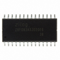
Z8F083ASJ020EG
Manufacturer Part Number
Z8F083ASJ020EG
Description
IC ENCORE XP MCU FLASH 8K 28SOIC
Manufacturer
Zilog
Series
Encore!®r
Datasheet
1.Z8F083ASJ020EG.pdf
(256 pages)
Specifications of Z8F083ASJ020EG
Core Processor
Z8
Core Size
8-Bit
Speed
20MHz
Peripherals
Brown-out Detect/Reset, LED, POR, PWM, WDT
Number Of I /o
23
Program Memory Size
8KB (8K x 8)
Program Memory Type
FLASH
Ram Size
256 x 8
Voltage - Supply (vcc/vdd)
2.7 V ~ 3.6 V
Data Converters
A/D 8x10b
Oscillator Type
Internal
Operating Temperature
-40°C ~ 105°C
Package / Case
28-SOIC (7.5mm Width)
Data Bus Width
8 bit
Data Ram Size
256 B
Maximum Clock Frequency
20 MHz
Number Of Programmable I/os
23
Number Of Timers
2
Maximum Operating Temperature
+ 105 C
Mounting Style
SMD/SMT
Minimum Operating Temperature
- 40 C
On-chip Adc
10 bit, 8 Channel
For Use With
770-1002 - ISP 4PORT ZILOG Z8 ENCORE! MCU269-4672 - KIT DEVELOPMENT F083A
Lead Free Status / RoHS Status
Lead free / RoHS Compliant
Eeprom Size
-
Connectivity
-
Lead Free Status / Rohs Status
Details
Other names
269-4558-5
Available stocks
Company
Part Number
Manufacturer
Quantity
Price
Company:

Part Number:
Z8F083ASJ020EG
Manufacturer:
Zilog
Quantity:
363


Operation
PS026308-1207
OCD Interface
Caution:
Figure 18. Interfacing the On-Chip Debugger’s DBG Pin with an RS-232 Interface (1)
The On-Chip Debugger uses the DBG pin for communication with an external host. This
one-pin interface is a bidirectional open-drain interface that transmits and receives data.
Data transmission is half-duplex, which means transmission and data retrieval cannot
occur simultaneously. The serial data on the DBG pin is sent using the standard
asynchronous data format defined in RS-232.This pin creates an interface between the Z8
Encore! F083A Series products and the serial port of a host PC using minimal external
hardware.Two different methods for connecting the DBG pin to an RS-232 interface are
displayed in
buffered implementation depicted in
connected to V
RS-232 TX
RS-232 RX
For operation of the On-Chip Debugger, all power pins (V
must be supplied with power, and all ground pins (V
properly grounded.
The
an external pull-up resistor to insure proper operation.
DBG
Figure 18
DD
pin is open-drain and must always be connected to V
through an external pull-up resistor.
Transceiver
and
RS-232
Figure 19
Figure 19
on page 135. The recommended method is the
Schottky
Diode
on page 135. The DBG pin must always be
VDD
10KOhm
Z8 Encore!
SS
DBG Pin
and AV
Product Specification
DD
DD
SS
and AV
®
) must be
On-Chip Debugger
through
F083A Series
DD
)
134
Related parts for Z8F083ASJ020EG
Image
Part Number
Description
Manufacturer
Datasheet
Request
R

Part Number:
Description:
Communication Controllers, ZILOG INTELLIGENT PERIPHERAL CONTROLLER (ZIP)
Manufacturer:
Zilog, Inc.
Datasheet:

Part Number:
Description:
KIT DEV FOR Z8 ENCORE 16K TO 64K
Manufacturer:
Zilog
Datasheet:

Part Number:
Description:
KIT DEV Z8 ENCORE XP 28-PIN
Manufacturer:
Zilog
Datasheet:

Part Number:
Description:
DEV KIT FOR Z8 ENCORE 8K/4K
Manufacturer:
Zilog
Datasheet:

Part Number:
Description:
KIT DEV Z8 ENCORE XP 28-PIN
Manufacturer:
Zilog
Datasheet:

Part Number:
Description:
DEV KIT FOR Z8 ENCORE 4K TO 8K
Manufacturer:
Zilog
Datasheet:
Part Number:
Description:
CMOS Z8 microcontroller. ROM 16 Kbytes, RAM 256 bytes, speed 16 MHz, 32 lines I/O, 3.0V to 5.5V
Manufacturer:
Zilog, Inc.
Datasheet:
Part Number:
Description:
Low-cost microcontroller. 512 bytes ROM, 61 bytes RAM, 8 MHz
Manufacturer:
Zilog, Inc.
Datasheet:
Part Number:
Description:
Z8 4K OTP Microcontroller
Manufacturer:
Zilog, Inc.
Datasheet:
Part Number:
Description:
CMOS SUPER8 ROMLESS MCU
Manufacturer:
Zilog, Inc.
Datasheet:
Part Number:
Description:
SL1866 CMOSZ8 OTP Microcontroller
Manufacturer:
Zilog, Inc.
Datasheet:
Part Number:
Description:
SL1866 CMOSZ8 OTP Microcontroller
Manufacturer:
Zilog, Inc.
Datasheet:
Part Number:
Description:
OTP (KB) = 1, RAM = 125, Speed = 12, I/O = 14, 8-bit Timers = 2, Comm Interfaces Other Features = Por, LV Protect, Voltage = 4.5-5.5V
Manufacturer:
Zilog, Inc.
Datasheet:
Part Number:
Description:
Manufacturer:
Zilog, Inc.
Datasheet: