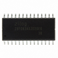
Z8F083ASJ020EG Zilog, Z8F083ASJ020EG Datasheet - Page 16

Z8F083ASJ020EG
Manufacturer Part Number
Z8F083ASJ020EG
Description
IC ENCORE XP MCU FLASH 8K 28SOIC
Manufacturer
Zilog
Series
Encore!®r
Datasheet
1.Z8F083ASJ020EG.pdf
(256 pages)
Specifications of Z8F083ASJ020EG
Core Processor
Z8
Core Size
8-Bit
Speed
20MHz
Peripherals
Brown-out Detect/Reset, LED, POR, PWM, WDT
Number Of I /o
23
Program Memory Size
8KB (8K x 8)
Program Memory Type
FLASH
Ram Size
256 x 8
Voltage - Supply (vcc/vdd)
2.7 V ~ 3.6 V
Data Converters
A/D 8x10b
Oscillator Type
Internal
Operating Temperature
-40°C ~ 105°C
Package / Case
28-SOIC (7.5mm Width)
Data Bus Width
8 bit
Data Ram Size
256 B
Maximum Clock Frequency
20 MHz
Number Of Programmable I/os
23
Number Of Timers
2
Maximum Operating Temperature
+ 105 C
Mounting Style
SMD/SMT
Minimum Operating Temperature
- 40 C
On-chip Adc
10 bit, 8 Channel
For Use With
770-1002 - ISP 4PORT ZILOG Z8 ENCORE! MCU269-4672 - KIT DEVELOPMENT F083A
Lead Free Status / RoHS Status
Lead free / RoHS Compliant
Eeprom Size
-
Connectivity
-
Lead Free Status / Rohs Status
Details
Other names
269-4558-5
Available stocks
Company
Part Number
Manufacturer
Quantity
Price
Company:
Part Number:
Z8F083ASJ020EG
Manufacturer:
Zilog
Quantity:
363
- Current page: 16 of 256
- Download datasheet (2Mb)
CPU and Peripheral Overview
PS026308-1207
eZ8 CPU Features
General Purpose Input/Output
Flash Controller
The eZ8 CPU, Zilog’s latest 8-bit CPU, meets the continuing demand for faster and more
code-efficient microcontrollers. The eZ8 CPU executes a superset of the original Z8
instruction set. The eZ8 CPU features include:
•
•
•
•
•
•
•
•
•
•
•
For more information regarding the eZ8 CPU, refer to eZ8 CPU User Manual available
for download at www.zilog.com.
The Z8 Encore! F083A Series features up to 23 port pins (Ports A–D) for general purpose
input/output (GPIO). The number of GPIO pins available is a function of package. Each
pin is individually programmable.
The Flash controller programs and erases the Flash memory. It also supports protection
against accidental programming and erasure.
Direct register-to-register architecture allows each register to function as an accumulator,
improving execution time and decreasing the required program memory.
Software stack allows much greater depth in subroutine calls and interrupts than hardware
stacks.
Compatible with existing Z8 CPU code.
Expanded internal Register File allows access up to 4 KB.
New instructions improve execution efficiency for code developed using high-level
programming languages, including C.
Pipelined instruction fetch and execute.
New instructions for improved performance including BIT, BSWAP, BTJ, CPC, LDC,
LDCI, LEA, MULT, and SRL
New instructions support 12-bit linear addressing of the Register File.
Up to10 MIPS operation.
C-compiler friendly.
Two to nine clock cycles per instruction.
Z8 Encore!
Product Specification
®
F083A Series
Overview
4
Related parts for Z8F083ASJ020EG
Image
Part Number
Description
Manufacturer
Datasheet
Request
R

Part Number:
Description:
Communication Controllers, ZILOG INTELLIGENT PERIPHERAL CONTROLLER (ZIP)
Manufacturer:
Zilog, Inc.
Datasheet:

Part Number:
Description:
KIT DEV FOR Z8 ENCORE 16K TO 64K
Manufacturer:
Zilog
Datasheet:

Part Number:
Description:
KIT DEV Z8 ENCORE XP 28-PIN
Manufacturer:
Zilog
Datasheet:

Part Number:
Description:
DEV KIT FOR Z8 ENCORE 8K/4K
Manufacturer:
Zilog
Datasheet:

Part Number:
Description:
KIT DEV Z8 ENCORE XP 28-PIN
Manufacturer:
Zilog
Datasheet:

Part Number:
Description:
DEV KIT FOR Z8 ENCORE 4K TO 8K
Manufacturer:
Zilog
Datasheet:

Part Number:
Description:
CMOS Z8 microcontroller. ROM 16 Kbytes, RAM 256 bytes, speed 16 MHz, 32 lines I/O, 3.0V to 5.5V
Manufacturer:
Zilog, Inc.
Datasheet:

Part Number:
Description:
Low-cost microcontroller. 512 bytes ROM, 61 bytes RAM, 8 MHz
Manufacturer:
Zilog, Inc.
Datasheet:

Part Number:
Description:
Z8 4K OTP Microcontroller
Manufacturer:
Zilog, Inc.
Datasheet:

Part Number:
Description:
CMOS SUPER8 ROMLESS MCU
Manufacturer:
Zilog, Inc.
Datasheet:

Part Number:
Description:
SL1866 CMOSZ8 OTP Microcontroller
Manufacturer:
Zilog, Inc.
Datasheet:

Part Number:
Description:
SL1866 CMOSZ8 OTP Microcontroller
Manufacturer:
Zilog, Inc.
Datasheet:

Part Number:
Description:
OTP (KB) = 1, RAM = 125, Speed = 12, I/O = 14, 8-bit Timers = 2, Comm Interfaces Other Features = Por, LV Protect, Voltage = 4.5-5.5V
Manufacturer:
Zilog, Inc.
Datasheet:

Part Number:
Description:
Manufacturer:
Zilog, Inc.
Datasheet:


