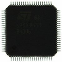
UPSD3422E-40U6 STMicroelectronics, UPSD3422E-40U6 Datasheet - Page 202

UPSD3422E-40U6
Manufacturer Part Number
UPSD3422E-40U6
Description
MCU 8BIT 8032 64KB FLASH 80TQFP
Manufacturer
STMicroelectronics
Series
µPSDr
Datasheet
1.UPSD3422EV-40U6.pdf
(300 pages)
Specifications of UPSD3422E-40U6
Core Processor
8032
Core Size
8-Bit
Speed
40MHz
Connectivity
I²C, IrDA, SPI, UART/USART, USB
Peripherals
LVD, POR, PWM, WDT
Number Of I /o
46
Program Memory Size
80KB (80K x 8)
Program Memory Type
FLASH
Ram Size
4K x 8
Voltage - Supply (vcc/vdd)
3 V ~ 5.5 V
Data Converters
A/D 8x10b
Oscillator Type
Internal
Operating Temperature
-40°C ~ 85°C
Package / Case
80-TQFP, 80-VQFP
For Use With
497-5577 - BOARD EVAL USB POWER SWITCH497-5518 - EVAL BOARD RFID READER
Lead Free Status / RoHS Status
Lead free / RoHS Compliant
Eeprom Size
-
Other names
497-4903
Available stocks
Company
Part Number
Manufacturer
Quantity
Price
Company:
Part Number:
UPSD3422E-40U6
Manufacturer:
STMicroelectronics
Quantity:
10 000
- Current page: 202 of 300
- Download datasheet (3Mb)
PSD module
28.2.6
Note:
202/300
from the Secondary Flash memory in program space. After the writing is complete, the Main
Flash can be “reclassified” back to program space, then execution can continue from the
new code in Main Flash memory. The mapping example of
operation.
Memory sector select rules
When defining sector select signals (FSx, CSBOOTx, RS0, CSIOP, PSELx) in PSDsoft
Express, the user must keep these rules in mind:
●
●
●
●
●
PSELx is for optional Peripheral I/O Mode on Port A.
●
Figure 68
Priority refers to which memory will ultimately produce a byte of data or code to the 8032
MCU for a given bus cycle. Any memory on a higher level can overlap and has priority over
any memory on a lower level. Memories on the same level must not overlap.
Example: FS0 is valid when the 8032 produces an address in the range of 8000h to BFFFh.
CSBOOT0 is valid from 8000h to 9FFFh. RS0 is valid from 8000h to 87FFh. Any address
from the 8032 in the range of RS0 always accesses the SRAM. Any address in the range of
CSBOOT0 greater than 87FFh (and less than 9FFFh) automatically addresses Secondary
Flash memory. Any address greater than 9FFFh accesses Main Flash memory. One-half of
the Main Flash memory segment and one-fourth of the Secondary Flash memory segment
cannot be accessed by the 8032.
Figure 68. PSD module memory priority
Main Flash and Secondary Flash memory sector select signals may not be larger than
their physical sector size as defined in
Any Main Flash memory sector select may not be mapped in the same address range
as another Main Flash sector select (cannot overlap segments of Main Flash on top of
each other).
Any Secondary Flash memory sector select may not be mapped in the same address
range as another Secondary Flash sector select (cannot overlap segments of
Secondary Flash on top of each other).
A Secondary Flash memory sector may overlap a Main Flash memory sector. In the
case of overlap, priority is given to the Secondary Flash memory sector.
SRAM, CSIOP, or PSELx may overlap any Flash memory sector. In the case of overlap,
priority is given to SRAM, CSIOP, or PSELx.
The address range for sector selects for SRAM, PSELx, and CSIOP must not overlap
each other as they have the same priority, causing contention if overlapped.
illustrates the priority scheme of the memory elements of the PSD module.
Highest priority
Lowest priority
Main Flash memory
Flash memory
Peripheral I/O
CSIOP, and
Secondary
Level 2
Level 3
Level 1
SRAM,
mode
UPSD3422, UPSD3433, UPSD3434, UPSD3454
Table 157 on page
AI02867E
Figure 67
193.
will accommodate this
Related parts for UPSD3422E-40U6
Image
Part Number
Description
Manufacturer
Datasheet
Request
R

Part Number:
Description:
Fast Turbo 8032 MCU with USB and Programmable Logic
Manufacturer:
STMICROELECTRONICS [STMicroelectronics]
Datasheet:

Part Number:
Description:
MCU 8BIT 8032 64KB FLASH 52TQFP
Manufacturer:
STMicroelectronics
Datasheet:

Part Number:
Description:
STMicroelectronics [RIPPLE-CARRY BINARY COUNTER/DIVIDERS]
Manufacturer:
STMicroelectronics
Datasheet:

Part Number:
Description:
STMicroelectronics [LIQUID-CRYSTAL DISPLAY DRIVERS]
Manufacturer:
STMicroelectronics
Datasheet:

Part Number:
Description:
BOARD EVAL FOR MEMS SENSORS
Manufacturer:
STMicroelectronics
Datasheet:

Part Number:
Description:
NPN TRANSISTOR POWER MODULE
Manufacturer:
STMicroelectronics
Datasheet:

Part Number:
Description:
TURBOSWITCH ULTRA-FAST HIGH VOLTAGE DIODE
Manufacturer:
STMicroelectronics
Datasheet:

Part Number:
Description:
Manufacturer:
STMicroelectronics
Datasheet:

Part Number:
Description:
DIODE / SCR MODULE
Manufacturer:
STMicroelectronics
Datasheet:

Part Number:
Description:
DIODE / SCR MODULE
Manufacturer:
STMicroelectronics
Datasheet:

Part Number:
Description:
Search -----> STE16N100
Manufacturer:
STMicroelectronics
Datasheet:

Part Number:
Description:
Search ---> STE53NA50
Manufacturer:
STMicroelectronics
Datasheet:


