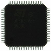
UPSD3422E-40U6 STMicroelectronics, UPSD3422E-40U6 Datasheet - Page 68

UPSD3422E-40U6
Manufacturer Part Number
UPSD3422E-40U6
Description
MCU 8BIT 8032 64KB FLASH 80TQFP
Manufacturer
STMicroelectronics
Series
µPSDr
Datasheet
1.UPSD3422EV-40U6.pdf
(300 pages)
Specifications of UPSD3422E-40U6
Core Processor
8032
Core Size
8-Bit
Speed
40MHz
Connectivity
I²C, IrDA, SPI, UART/USART, USB
Peripherals
LVD, POR, PWM, WDT
Number Of I /o
46
Program Memory Size
80KB (80K x 8)
Program Memory Type
FLASH
Ram Size
4K x 8
Voltage - Supply (vcc/vdd)
3 V ~ 5.5 V
Data Converters
A/D 8x10b
Oscillator Type
Internal
Operating Temperature
-40°C ~ 85°C
Package / Case
80-TQFP, 80-VQFP
For Use With
497-5577 - BOARD EVAL USB POWER SWITCH497-5518 - EVAL BOARD RFID READER
Lead Free Status / RoHS Status
Lead free / RoHS Compliant
Eeprom Size
-
Other names
497-4903
Available stocks
Company
Part Number
Manufacturer
Quantity
Price
Company:
Part Number:
UPSD3422E-40U6
Manufacturer:
STMicroelectronics
Quantity:
10 000
- Current page: 68 of 300
- Download datasheet (3Mb)
MCU clock generation
14
14.1
14.2
14.2.1
68/300
MCU clock generation
Internal system clocks generated by the clock generation unit are derived from the signal,
XTAL1, shown in
external crystal or oscillator device. The SFR named CCON0
the clock generation unit.
There are two clock signals produced by the clock generation unit:
●
●
MCU_CLK
This clock drives the 8032 MCU core and the Watchdog Timer (WDT). The frequency of
MCU_CLK is equal to f
Figure
The new frequency is available immediately after the CPUPS[2:0] bits are written. The final
frequency of MCU_CLK is f
MCU_CLK is blocked by either bit, PD or IDL, in the SFR named PCON during MCU Power-
down mode or Idle mode respectively.
MCU_CLK clock can be further divided as required for use in the WDT. See details of the
WDT in
PERIPH_CLK
This clock drives all the UPSD34xx peripherals except the WDT. The Frequency of
PERIPH_CLK is always f
PERIPH_CLK to scale it appropriately for use.
PERIPH_CLK runs at all times except when blocked by the PD bit in the SFR named PCON
during MCU Power-down mode.
JTAG interface clock
The JTAG interface for ISP and for Debugging uses the externally supplied JTAG clock,
coming in on pin TCK. This means the JTAG ISP interface is always available, and the JTAG
Debug interface is available when enabled, even during MCU Idle mode and Power-down
mode.
However, since the MCU participates in the JTAG debug process, and MCU_CLK is halted
during Idle and Power-down modes, the majority of debug functions are not available during
these low power modes. But the JTAG debug interface is capable of executing a reset
command while in these low power modes, which will exit back to normal operating mode
where all debug commands are available again.
The CCON0 SFR contains a bit, DBGCE, which enables the breakpoint comparators inside
the JTAG Debug Unit when set. DBGCE is set by default after reset, and firmware may clear
this bit at run-time. Disabling these comparators will reduce current consumption on the
MCU module, and it is recommended to do so if the Debug Unit will not be used (such as in
the production version of an end-product).
MCU_CLK
PERIPH_CLK
13. The bits CPUPS[2:0] select one of eight different divisors, ranging from 2 to 2048.
Section 19: Supervisory functions on page
Figure
OSC
13. XTAL1 has a frequency f
OSC
MCU
by default, but it can be divided by as much as 2048, shown in
. Each of the peripherals can independently divide
.
UPSD3422, UPSD3433, UPSD3434, UPSD3454
91.
OSC
, which comes directly from the
(Table 27 on page
70) controls
Related parts for UPSD3422E-40U6
Image
Part Number
Description
Manufacturer
Datasheet
Request
R

Part Number:
Description:
Fast Turbo 8032 MCU with USB and Programmable Logic
Manufacturer:
STMICROELECTRONICS [STMicroelectronics]
Datasheet:

Part Number:
Description:
MCU 8BIT 8032 64KB FLASH 52TQFP
Manufacturer:
STMicroelectronics
Datasheet:

Part Number:
Description:
STMicroelectronics [RIPPLE-CARRY BINARY COUNTER/DIVIDERS]
Manufacturer:
STMicroelectronics
Datasheet:

Part Number:
Description:
STMicroelectronics [LIQUID-CRYSTAL DISPLAY DRIVERS]
Manufacturer:
STMicroelectronics
Datasheet:

Part Number:
Description:
BOARD EVAL FOR MEMS SENSORS
Manufacturer:
STMicroelectronics
Datasheet:

Part Number:
Description:
NPN TRANSISTOR POWER MODULE
Manufacturer:
STMicroelectronics
Datasheet:

Part Number:
Description:
TURBOSWITCH ULTRA-FAST HIGH VOLTAGE DIODE
Manufacturer:
STMicroelectronics
Datasheet:

Part Number:
Description:
Manufacturer:
STMicroelectronics
Datasheet:

Part Number:
Description:
DIODE / SCR MODULE
Manufacturer:
STMicroelectronics
Datasheet:

Part Number:
Description:
DIODE / SCR MODULE
Manufacturer:
STMicroelectronics
Datasheet:

Part Number:
Description:
Search -----> STE16N100
Manufacturer:
STMicroelectronics
Datasheet:

Part Number:
Description:
Search ---> STE53NA50
Manufacturer:
STMicroelectronics
Datasheet:


