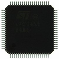
UPSD3422E-40U6 STMicroelectronics, UPSD3422E-40U6 Datasheet - Page 219

UPSD3422E-40U6
Manufacturer Part Number
UPSD3422E-40U6
Description
MCU 8BIT 8032 64KB FLASH 80TQFP
Manufacturer
STMicroelectronics
Series
µPSDr
Datasheet
1.UPSD3422EV-40U6.pdf
(300 pages)
Specifications of UPSD3422E-40U6
Core Processor
8032
Core Size
8-Bit
Speed
40MHz
Connectivity
I²C, IrDA, SPI, UART/USART, USB
Peripherals
LVD, POR, PWM, WDT
Number Of I /o
46
Program Memory Size
80KB (80K x 8)
Program Memory Type
FLASH
Ram Size
4K x 8
Voltage - Supply (vcc/vdd)
3 V ~ 5.5 V
Data Converters
A/D 8x10b
Oscillator Type
Internal
Operating Temperature
-40°C ~ 85°C
Package / Case
80-TQFP, 80-VQFP
For Use With
497-5577 - BOARD EVAL USB POWER SWITCH497-5518 - EVAL BOARD RFID READER
Lead Free Status / RoHS Status
Lead free / RoHS Compliant
Eeprom Size
-
Other names
497-4903
Available stocks
Company
Part Number
Manufacturer
Quantity
Price
Company:
Part Number:
UPSD3422E-40U6
Manufacturer:
STMicroelectronics
Quantity:
10 000
- Current page: 219 of 300
- Download datasheet (3Mb)
UPSD3422, UPSD3433, UPSD3434, UPSD3454
28.5.25
memory contents through its 8-bit data bus even while the security bit is set. The 8032 can
read the status of the security bit at run-time (but it cannot change it) by reading the csiop
register defined in
Table 165. Main Flash memory protection register definition (address = csiop +
1. Bit definitions:
Table 166. Secondary Flash memory protection/security register definition (csiop +
1. Sec<i>_Prot 1 = Flash memory sector <i> is write protected, 0 = Flash memory sector <i> is not write
2. Security_Bit = 1, device is secured, 0 = not secured.
PLDs
The PSD module contains two PLDs: the Decode PLD (DPLD), and the General PLD
(GPLD), as shown in
signal bus, and additionally, the GPLD is connected to the 8032 data bus.
PLD logic is specified using PSDsoft Express and programmed into the PSD module using
the JTAG ISP channel. PLD logic is non-volatile and available at power-up. PLDs may not be
programmed by the 8032. The PLDs have selectable levels of performance and power
consumption.
The DPLD performs address decoding, and generates select signals for internal and
external components, such as memory, registers, and I/O ports. The DPLD can generate
External Chip-Select (ECS1-ECS2) signals on Port D.
The GPLD can be used for logic functions, such as loadable counters and shift registers,
state machines, encoding and decoding logic. These logic functions can be constructed
from a combination of 16 Output Macrocells (OMC), 20 Input Macrocells (IMC), and the
AND-OR Array.
Routing of the 16 OMCs outputs can be divided between pins on three Ports A, B, or C by
the OMC Allocator as shown in
routed to pins on Port A or Port B and are named MCELLAB0-MCELLAB7. The other eight
OMCs to be routed to pins on Port B or Port C and are named MCELLBC0-MCELLBC7.
This routing depends on the pin number assignments that are specified in PSDsoft Express
for “PLD Outputs” in the Pin Definition section. OMC outputs can also be routed internally
(not to pins) used as buried nodes to create shifters, counters, etc.
The AND-OR Array is used to form product terms. These product terms are configured from
the logic definitions entered in PSDsoft Express. A PLD Input Bus consisting of 69 signals is
connected to both PLDs. Input signals are shown in
compliment versions of each of these signals are available at inputs to each PLD.
Sec7_Prot Sec6_Prot Sec5_Prot Sec4_Prot Sec3_Prot Sec2_Prot Sec1_Prot Sec0_Prot
Security_Bit
Sec<i>_Prot 1 = Flash memory sector <i> is write protected, 0 = Flash memory sector <i> is not write
protected.
protected.
Bit 7
Bit 7
(2)
offset C0h)
offset C2h)
Bit 6
not used
Bit 6
Table
Figure 73 on page
166.
(1)
not used
Bit 5
Bit 5
Figure 77 on page
not used
Bit 4
Bit 4
221. Both PLDs are fed by a common PLD input
Sec3_Prot Sec2_Prot Sec1_Prot Sec0_Prot
Bit 3
Bit 3
227. Eight of the 16 OMCs that can be
Table
(1)
167, both the true and
Bit 2
Bit 2
(1)
Bit 1
Bit 1
(1)
PSD module
Bit 0
Bit 0
219/300
(1)
Related parts for UPSD3422E-40U6
Image
Part Number
Description
Manufacturer
Datasheet
Request
R

Part Number:
Description:
Fast Turbo 8032 MCU with USB and Programmable Logic
Manufacturer:
STMICROELECTRONICS [STMicroelectronics]
Datasheet:

Part Number:
Description:
MCU 8BIT 8032 64KB FLASH 52TQFP
Manufacturer:
STMicroelectronics
Datasheet:

Part Number:
Description:
STMicroelectronics [RIPPLE-CARRY BINARY COUNTER/DIVIDERS]
Manufacturer:
STMicroelectronics
Datasheet:

Part Number:
Description:
STMicroelectronics [LIQUID-CRYSTAL DISPLAY DRIVERS]
Manufacturer:
STMicroelectronics
Datasheet:

Part Number:
Description:
BOARD EVAL FOR MEMS SENSORS
Manufacturer:
STMicroelectronics
Datasheet:

Part Number:
Description:
NPN TRANSISTOR POWER MODULE
Manufacturer:
STMicroelectronics
Datasheet:

Part Number:
Description:
TURBOSWITCH ULTRA-FAST HIGH VOLTAGE DIODE
Manufacturer:
STMicroelectronics
Datasheet:

Part Number:
Description:
Manufacturer:
STMicroelectronics
Datasheet:

Part Number:
Description:
DIODE / SCR MODULE
Manufacturer:
STMicroelectronics
Datasheet:

Part Number:
Description:
DIODE / SCR MODULE
Manufacturer:
STMicroelectronics
Datasheet:

Part Number:
Description:
Search -----> STE16N100
Manufacturer:
STMicroelectronics
Datasheet:

Part Number:
Description:
Search ---> STE53NA50
Manufacturer:
STMicroelectronics
Datasheet:


