MC9S08QD4VSC Freescale Semiconductor, MC9S08QD4VSC Datasheet - Page 12
MC9S08QD4VSC
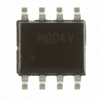
Manufacturer Part Number
MC9S08QD4VSC
Description
IC MCU 4K FLASH 256RAM 8-SOIC
Manufacturer
Freescale Semiconductor
Series
HCS08r
Specifications of MC9S08QD4VSC
Core Processor
HCS08
Core Size
8-Bit
Speed
10MHz
Peripherals
LVD, POR, PWM, WDT
Number Of I /o
4
Program Memory Size
4KB (4K x 8)
Program Memory Type
FLASH
Ram Size
256 x 8
Voltage - Supply (vcc/vdd)
2.7 V ~ 5.5 V
Data Converters
A/D 4x10b
Oscillator Type
Internal
Operating Temperature
-40°C ~ 125°C
Package / Case
8-SOIC (3.9mm Width)
Processor Series
S08QD
Core
HCS08
Data Bus Width
8 bit
Data Ram Size
256 B
Interface Type
I2C, SCI, SPI
Maximum Clock Frequency
8 MHz
Number Of Programmable I/os
4
Number Of Timers
3
Operating Supply Voltage
2.7 V to 5.5 V
Maximum Operating Temperature
+ 105 C
Mounting Style
SMD/SMT
3rd Party Development Tools
EWS08
Development Tools By Supplier
DEMO9S08QD4
Minimum Operating Temperature
- 40 C
On-chip Adc
4-ch x 10-bit
Cpu Family
HCS08
Device Core Size
8b
Frequency (max)
8MHz
Total Internal Ram Size
256Byte
# I/os (max)
4
Number Of Timers - General Purpose
3
Operating Supply Voltage (typ)
3.3/5V
Operating Supply Voltage (max)
5.5V
Operating Supply Voltage (min)
2.7V
Instruction Set Architecture
CISC
Operating Temp Range
-40C to 105C
Operating Temperature Classification
Industrial
Mounting
Surface Mount
Pin Count
8
Package Type
SOIC N
For Use With
DEMO9S08QD4 - BOARD DEMO FOR MC9S08QD FAMILY
Lead Free Status / RoHS Status
Lead free / RoHS Compliant
Eeprom Size
-
Connectivity
-
Lead Free Status / Rohs Status
Lead free / RoHS Compliant
Available stocks
Company
Part Number
Manufacturer
Quantity
Price


8.4
8.5
8.6
9.1
9.2
9.3
9.4
12
Functional Description ..................................................................................................................108
Initialization Information ..............................................................................................................113
Application Information ................................................................................................................115
Introduction ...................................................................................................................................121
External Signal Description ..........................................................................................................125
Register Definition ........................................................................................................................125
Functional Description ..................................................................................................................128
8.3.2 Status and Control Register 2 (ADCSC2) ......................................................................101
8.3.3 Data Result High Register (ADCRH) .............................................................................102
8.3.4 Data Result Low Register (ADCRL) ..............................................................................102
8.3.5 Compare Value High Register (ADCCVH) ....................................................................103
8.3.6 Compare Value Low Register (ADCCVL) .....................................................................103
8.3.7 Configuration Register (ADCCFG) ................................................................................103
8.3.8 Pin Control 1 Register (APCTL1) ..................................................................................105
8.3.9 Pin Control 2 Register (APCTL2) ..................................................................................106
8.3.10 Pin Control 3 Register (APCTL3) ..................................................................................107
8.4.1 Clock Select and Divide Control ....................................................................................108
8.4.2 Input Select and Pin Control ...........................................................................................109
8.4.3 Hardware Trigger ............................................................................................................109
8.4.4 Conversion Control .........................................................................................................109
8.4.5 Automatic Compare Function .........................................................................................112
8.4.6 MCU Wait Mode Operation ............................................................................................112
8.4.7 MCU Stop3 Mode Operation ..........................................................................................112
8.4.8 MCU Stop1 and Stop2 Mode Operation .........................................................................113
8.5.1 ADC Module Initialization Example .............................................................................113
8.6.1 External Pins and Routing ..............................................................................................115
8.6.2 Sources of Error ..............................................................................................................117
9.1.1 ICS Configuration Information .......................................................................................121
9.1.2 Features ...........................................................................................................................123
9.1.3 Modes of Operation ........................................................................................................123
9.1.4 Block Diagram ................................................................................................................124
9.3.1 ICS Control Register 1 (ICSC1) .....................................................................................125
9.3.2 ICS Control Register 2 (ICSC2) .....................................................................................126
9.3.3 ICS Trim Register (ICSTRM) .........................................................................................127
9.3.4 ICS Status and Control (ICSSC) .....................................................................................127
9.4.1 Operational Modes ..........................................................................................................128
9.4.2 Mode Switching ..............................................................................................................130
9.4.3 Bus Frequency Divider ...................................................................................................130
9.4.4 Low Power Bit Usage .....................................................................................................131
9.4.5 Internal Reference Clock ................................................................................................131
9.4.6 Optional External Reference Clock ................................................................................131
9.4.7 Fixed Frequency Clock ...................................................................................................132
Internal Clock Source (S08ICSV1)
MC9S08QD4 Series MCU Data Sheet, Rev. 6
Chapter 9
Freescale Semiconductor
Related parts for MC9S08QD4VSC
Image
Part Number
Description
Manufacturer
Datasheet
Request
R

Part Number:
Description:
Manufacturer:
Freescale Semiconductor, Inc
Datasheet:
Part Number:
Description:
Manufacturer:
Freescale Semiconductor, Inc
Datasheet:
Part Number:
Description:
Manufacturer:
Freescale Semiconductor, Inc
Datasheet:
Part Number:
Description:
Manufacturer:
Freescale Semiconductor, Inc
Datasheet:
Part Number:
Description:
Manufacturer:
Freescale Semiconductor, Inc
Datasheet:
Part Number:
Description:
Manufacturer:
Freescale Semiconductor, Inc
Datasheet:
Part Number:
Description:
Manufacturer:
Freescale Semiconductor, Inc
Datasheet:
Part Number:
Description:
Manufacturer:
Freescale Semiconductor, Inc
Datasheet:
Part Number:
Description:
Manufacturer:
Freescale Semiconductor, Inc
Datasheet:
Part Number:
Description:
Manufacturer:
Freescale Semiconductor, Inc
Datasheet:
Part Number:
Description:
Manufacturer:
Freescale Semiconductor, Inc
Datasheet:
Part Number:
Description:
Manufacturer:
Freescale Semiconductor, Inc
Datasheet:
Part Number:
Description:
Manufacturer:
Freescale Semiconductor, Inc
Datasheet:
Part Number:
Description:
Manufacturer:
Freescale Semiconductor, Inc
Datasheet:
Part Number:
Description:
Manufacturer:
Freescale Semiconductor, Inc
Datasheet: