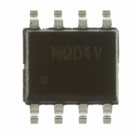
MC9S08QD4VSC Freescale Semiconductor, MC9S08QD4VSC Datasheet - Page 186

MC9S08QD4VSC
Manufacturer Part Number
MC9S08QD4VSC
Description
IC MCU 4K FLASH 256RAM 8-SOIC
Manufacturer
Freescale Semiconductor
Series
HCS08r
Specifications of MC9S08QD4VSC
Core Processor
HCS08
Core Size
8-Bit
Speed
10MHz
Peripherals
LVD, POR, PWM, WDT
Number Of I /o
4
Program Memory Size
4KB (4K x 8)
Program Memory Type
FLASH
Ram Size
256 x 8
Voltage - Supply (vcc/vdd)
2.7 V ~ 5.5 V
Data Converters
A/D 4x10b
Oscillator Type
Internal
Operating Temperature
-40°C ~ 125°C
Package / Case
8-SOIC (3.9mm Width)
Processor Series
S08QD
Core
HCS08
Data Bus Width
8 bit
Data Ram Size
256 B
Interface Type
I2C, SCI, SPI
Maximum Clock Frequency
8 MHz
Number Of Programmable I/os
4
Number Of Timers
3
Operating Supply Voltage
2.7 V to 5.5 V
Maximum Operating Temperature
+ 105 C
Mounting Style
SMD/SMT
3rd Party Development Tools
EWS08
Development Tools By Supplier
DEMO9S08QD4
Minimum Operating Temperature
- 40 C
On-chip Adc
4-ch x 10-bit
Cpu Family
HCS08
Device Core Size
8b
Frequency (max)
8MHz
Total Internal Ram Size
256Byte
# I/os (max)
4
Number Of Timers - General Purpose
3
Operating Supply Voltage (typ)
3.3/5V
Operating Supply Voltage (max)
5.5V
Operating Supply Voltage (min)
2.7V
Instruction Set Architecture
CISC
Operating Temp Range
-40C to 105C
Operating Temperature Classification
Industrial
Mounting
Surface Mount
Pin Count
8
Package Type
SOIC N
For Use With
DEMO9S08QD4 - BOARD DEMO FOR MC9S08QD FAMILY
Lead Free Status / RoHS Status
Lead free / RoHS Compliant
Eeprom Size
-
Connectivity
-
Lead Free Status / Rohs Status
Lead free / RoHS Compliant
Available stocks
Company
Part Number
Manufacturer
Quantity
Price
Appendix A Electrical Characteristics
A.8
This section describes AC timing characteristics for each peripheral system.
A.8.1
1
2
3
4
5
186
Bus frequency (t
Real-time interrupt internal oscillator period
External reset pulse width
IRQ pulse width
KBIPx pulse width
Port rise and fall time (load = 50 pF)
BKGD/MS setup time after issuing background debug force
reset to enter user or BDM modes
BKGD/MS hold time after issuing background debug force
reset to enter user or BDM modes
Data in Typical column was characterized at 3.0 V, 25°C.
This is the shortest pulse that is guaranteed to be recognized.
This is the minimum pulse width that is guaranteed to pass through the pin synchronization circuitry. Shorter pulses may or
may not be recognized. In stop mode, the synchronizer is bypassed so shorter pulses can be recognized in that case.
Timing is shown with respect to 20% V
To enter BDM mode following a POR, BKGD/MS must be held low during the power-up and for a hold time of t
rises above V
Slew rate control enabled (PTxSE = 1)
Slew rate control disabled (PTxSE = 0)
Asynchronous path
Synchronous path
Asynchronous path
Synchronous path
AC Characteristics
Control Timing
LVD
cyc
.
= 1/f
3
3
2
2
RESET PIN
Bus
Parameter
2
)
5
4
MC9S08QD4 Series MCU Data Sheet, Rev. 6
DD
and 80% V
Figure A-12. Reset Timing
Table A-8. Control Timing
DD
levels. Temperature range –40°C to 125°C.
t
t
t
Symbol
ILIH,
ILIH,
Rise
t
t
MSSU
t
t
f
extrst
t
MSH
extrst
Bus
RTI
, t
t
t
IHIL
IHIL
Fall
1.5 t
1.5 t
Min
700
100
100
100
500
100
—
—
1
cyc
cyc
Typical
30
—
—
—
—
—
—
—
3
1
Freescale Semiconductor
1300
Max
—
—
—
—
—
—
—
8
MSH
after V
MHz
Unit
μs
ns
ns
ns
ns
ns
μs
DD


