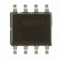
MC9S08QD4VSC Freescale Semiconductor, MC9S08QD4VSC Datasheet - Page 159

MC9S08QD4VSC
Manufacturer Part Number
MC9S08QD4VSC
Description
IC MCU 4K FLASH 256RAM 8-SOIC
Manufacturer
Freescale Semiconductor
Series
HCS08r
Specifications of MC9S08QD4VSC
Core Processor
HCS08
Core Size
8-Bit
Speed
10MHz
Peripherals
LVD, POR, PWM, WDT
Number Of I /o
4
Program Memory Size
4KB (4K x 8)
Program Memory Type
FLASH
Ram Size
256 x 8
Voltage - Supply (vcc/vdd)
2.7 V ~ 5.5 V
Data Converters
A/D 4x10b
Oscillator Type
Internal
Operating Temperature
-40°C ~ 125°C
Package / Case
8-SOIC (3.9mm Width)
Processor Series
S08QD
Core
HCS08
Data Bus Width
8 bit
Data Ram Size
256 B
Interface Type
I2C, SCI, SPI
Maximum Clock Frequency
8 MHz
Number Of Programmable I/os
4
Number Of Timers
3
Operating Supply Voltage
2.7 V to 5.5 V
Maximum Operating Temperature
+ 105 C
Mounting Style
SMD/SMT
3rd Party Development Tools
EWS08
Development Tools By Supplier
DEMO9S08QD4
Minimum Operating Temperature
- 40 C
On-chip Adc
4-ch x 10-bit
Cpu Family
HCS08
Device Core Size
8b
Frequency (max)
8MHz
Total Internal Ram Size
256Byte
# I/os (max)
4
Number Of Timers - General Purpose
3
Operating Supply Voltage (typ)
3.3/5V
Operating Supply Voltage (max)
5.5V
Operating Supply Voltage (min)
2.7V
Instruction Set Architecture
CISC
Operating Temp Range
-40C to 105C
Operating Temperature Classification
Industrial
Mounting
Surface Mount
Pin Count
8
Package Type
SOIC N
For Use With
DEMO9S08QD4 - BOARD DEMO FOR MC9S08QD FAMILY
Lead Free Status / RoHS Status
Lead free / RoHS Compliant
Eeprom Size
-
Connectivity
-
Lead Free Status / Rohs Status
Lead free / RoHS Compliant
Available stocks
Company
Part Number
Manufacturer
Quantity
Price
Chapter 12
Development Support
12.1
Development support systems in the HCS08 include the background debug controller (BDC). The BDC
provides a single-wire debug interface to the target MCU that provides a convenient interface for
programming the on-chip flash and other nonvolatile memories. The BDC is also the primary debug
interface for development and allows non-intrusive access to memory data and traditional debug features
such as CPU register modify, breakpoints, and single instruction trace commands.
In the HCS08 Family, address and data bus signals are not available on external pins (not even in test
modes). Debug is done through commands fed into the target MCU via the single-wire background debug
interface. The debug module provides a means to selectively trigger and capture bus information so an
external development system can reconstruct what happened inside the MCU on a cycle-by-cycle basis
without having external access to the address and data signals.
12.1.1
The method for forcing active background mode depends on the specific HCS08 derivative. For the
MC9S08QD4 series, you can force active background mode by holding the BKGD pin low as the MCU
exits the reset condition independent of what caused the reset. If no debug pod is connected to the BKGD
pin, the MCU will always reset into normal operating mode.
12.1.2
The alternative BDC clock source for MC9S08QD4 series is the ICGCLK. See
Source
Freescale Semiconductor
(S08ICSV1),” for more information about ICGCLK and how to select clock sources.
Introduction
Forcing Active Background
Module Configuration
MC9S08QD4 Series MCU Data Sheet, Rev. 6
Chapter 9, “Internal Clock
159


