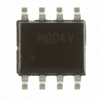
MC9S08QD4VSC Freescale Semiconductor, MC9S08QD4VSC Datasheet - Page 21

MC9S08QD4VSC
Manufacturer Part Number
MC9S08QD4VSC
Description
IC MCU 4K FLASH 256RAM 8-SOIC
Manufacturer
Freescale Semiconductor
Series
HCS08r
Specifications of MC9S08QD4VSC
Core Processor
HCS08
Core Size
8-Bit
Speed
10MHz
Peripherals
LVD, POR, PWM, WDT
Number Of I /o
4
Program Memory Size
4KB (4K x 8)
Program Memory Type
FLASH
Ram Size
256 x 8
Voltage - Supply (vcc/vdd)
2.7 V ~ 5.5 V
Data Converters
A/D 4x10b
Oscillator Type
Internal
Operating Temperature
-40°C ~ 125°C
Package / Case
8-SOIC (3.9mm Width)
Processor Series
S08QD
Core
HCS08
Data Bus Width
8 bit
Data Ram Size
256 B
Interface Type
I2C, SCI, SPI
Maximum Clock Frequency
8 MHz
Number Of Programmable I/os
4
Number Of Timers
3
Operating Supply Voltage
2.7 V to 5.5 V
Maximum Operating Temperature
+ 105 C
Mounting Style
SMD/SMT
3rd Party Development Tools
EWS08
Development Tools By Supplier
DEMO9S08QD4
Minimum Operating Temperature
- 40 C
On-chip Adc
4-ch x 10-bit
Cpu Family
HCS08
Device Core Size
8b
Frequency (max)
8MHz
Total Internal Ram Size
256Byte
# I/os (max)
4
Number Of Timers - General Purpose
3
Operating Supply Voltage (typ)
3.3/5V
Operating Supply Voltage (max)
5.5V
Operating Supply Voltage (min)
2.7V
Instruction Set Architecture
CISC
Operating Temp Range
-40C to 105C
Operating Temperature Classification
Industrial
Mounting
Surface Mount
Pin Count
8
Package Type
SOIC N
For Use With
DEMO9S08QD4 - BOARD DEMO FOR MC9S08QD FAMILY
Lead Free Status / RoHS Status
Lead free / RoHS Compliant
Eeprom Size
-
Connectivity
-
Lead Free Status / Rohs Status
Lead free / RoHS Compliant
Available stocks
Company
Part Number
Manufacturer
Quantity
Price
2.2.2
Out of reset the MCU uses an internally generated clock provided by the internal clock source (ICS)
module. The internal frequency is nominally 16 MHz and the default ICS settings will provide for a 4 MHz
bus out of reset. For more information on the ICS, see the
2.2.3
After a power-on reset (POR) into user mode, the PTA5/TPM2CH0I/IRQ/RESET pin defaults to a
general-purpose input port pin, PTA5. Setting RSTPE in SOPT1 configures the pin to be the RESET input
pin. Once configured as RESET, the pin will remain RESET until the next POR. The RESET pin can be
used to reset the MCU from an external source when the pin is driven low. When enabled as the RESET
pin (RSTPE = 1), an internal pullup device is automatically enabled.
After a POR into active background mode, the PTA5/TPM2CH0I/IRQ/RESET pin defaults to the RESET
pin.
When TPM2 is configured for input capture, the pin will be the input capture pin TPM2CH0I.
2.2.4
During a power-on-reset (POR) or background debug force reset (see
Debug Force Reset Register
functions as a mode select pin. Immediately after any reset, the pin functions as the background pin and
can be used for background debug communication. When enabled as the BKGD/MS pin (BKGDPE = 1),
an internal pullup device is automatically enabled.
The background debug communication function is enabled when BKGDPE in SOPT1 is set. BKGDPE is
set following any reset of the MCU and must be cleared to use the PTA4/TPM2CH0O/BKGD/MS pins
alternative pin functions.
If nothing is connected to this pin, the MCU will enter normal operating mode at the rising edge of the
internal reset after a POR or force BDC reset. If a debug system is connected to the 6-pin standard
background debug header, it can hold BKGD/MS low during a POR or immediately after issuing a
background debug force reset, which will force the MCU to active background mode.
The BKGD pin is used primarily for background debug controller (BDC) communications using a custom
protocol that uses 16 clock cycles of the target MCU’s BDC clock per bit time. The target MCU’s BDC
clock could be as fast as the maximum bus clock rate, so there must never be any significant capacitance
connected to the BKGD/MS pin that could interfere with background serial communications.
Freescale Semiconductor
Oscillator
Reset (Input Only)
Background / Mode Select (BKGD/MS)
This pin does not contain a clamp diode to V
above V
The voltage measured on the internally pulled up RESET pin may be as low
as V
DD
– 0.7 V. The internal gates connected to this pin are pulled to V
DD
.
(SBDFR)” for more information), the PTA4/TPM2CH0O/BKGD/MS pin
MC9S08QD4 Series MCU Data Sheet, Rev. 6
NOTE
Internal Clock Source
DD
and must not be driven
Section 5.8.3, “System Background
Chapter 2 External Signal Description
chapter.
DD
.
21


