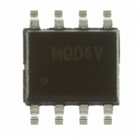
MC9S08QD4VSC Freescale Semiconductor, MC9S08QD4VSC Datasheet - Page 68

MC9S08QD4VSC
Manufacturer Part Number
MC9S08QD4VSC
Description
IC MCU 4K FLASH 256RAM 8-SOIC
Manufacturer
Freescale Semiconductor
Series
HCS08r
Specifications of MC9S08QD4VSC
Core Processor
HCS08
Core Size
8-Bit
Speed
10MHz
Peripherals
LVD, POR, PWM, WDT
Number Of I /o
4
Program Memory Size
4KB (4K x 8)
Program Memory Type
FLASH
Ram Size
256 x 8
Voltage - Supply (vcc/vdd)
2.7 V ~ 5.5 V
Data Converters
A/D 4x10b
Oscillator Type
Internal
Operating Temperature
-40°C ~ 125°C
Package / Case
8-SOIC (3.9mm Width)
Processor Series
S08QD
Core
HCS08
Data Bus Width
8 bit
Data Ram Size
256 B
Interface Type
I2C, SCI, SPI
Maximum Clock Frequency
8 MHz
Number Of Programmable I/os
4
Number Of Timers
3
Operating Supply Voltage
2.7 V to 5.5 V
Maximum Operating Temperature
+ 105 C
Mounting Style
SMD/SMT
3rd Party Development Tools
EWS08
Development Tools By Supplier
DEMO9S08QD4
Minimum Operating Temperature
- 40 C
On-chip Adc
4-ch x 10-bit
Cpu Family
HCS08
Device Core Size
8b
Frequency (max)
8MHz
Total Internal Ram Size
256Byte
# I/os (max)
4
Number Of Timers - General Purpose
3
Operating Supply Voltage (typ)
3.3/5V
Operating Supply Voltage (max)
5.5V
Operating Supply Voltage (min)
2.7V
Instruction Set Architecture
CISC
Operating Temp Range
-40C to 105C
Operating Temperature Classification
Industrial
Mounting
Surface Mount
Pin Count
8
Package Type
SOIC N
For Use With
DEMO9S08QD4 - BOARD DEMO FOR MC9S08QD FAMILY
Lead Free Status / RoHS Status
Lead free / RoHS Compliant
Eeprom Size
-
Connectivity
-
Lead Free Status / Rohs Status
Lead free / RoHS Compliant
Available stocks
Company
Part Number
Manufacturer
Quantity
Price
Chapter 6 Parallel Input/Output Control
The data direction control bit (PTxDDn) determines whether the output buffer for the associated pin is
enabled, and also controls the source for port data register reads. The input buffer for the associated pin is
always enabled unless the pin is enabled as an analog function or is an output-only pin.
When a shared digital function is enabled for a pin, the output buffer is controlled by the shared function.
However, the data direction register bit will continue to control the source for reads of the port data register.
When a shared analog function is enabled for a pin, both the input and output buffers are disabled. A value
of 0 is read for any port data bit where the bit is an input (PTxDDn = 0) and the input buffer is disabled. In
general, whenever a pin is shared with both an alternate digital function and an analog function, the analog
function has priority such that if both the digital and analog functions are enabled, the analog function
controls the pin.
It is a good programming practice to write to the port data register before changing the direction of a port
pin to become an output. This ensures that the pin will not be driven momentarily with an old data value
that happened to be in the port data register.
6.2
Associated with the parallel I/O ports is a set of registers located in the high-page register space that
operate independently of the parallel I/O registers. These registers are used to control pullups, slew rate
and drive strength for the pins.
6.3
Pin behavior following execution of a STOP instruction depends on the stop mode that is entered. An
explanation of pin behavior for the various stop modes follows:
68
Pin Control — Pullup, Slew Rate and Drive Strength
Pin Behavior in Stop Modes
Port Read
BUSCLK
Data
MC9S08QD4 Series MCU Data Sheet, Rev. 6
Figure 6-1. Parallel I/O Block Diagram
PTxDDn
D
D
PTxDn
Q
Q
1
0
Synchronizer
Output Enable
Output Data
Freescale Semiconductor
Input Data


