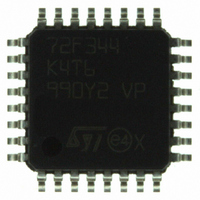
ST72F344K4T6 STMicroelectronics, ST72F344K4T6 Datasheet - Page 116

ST72F344K4T6
Manufacturer Part Number
ST72F344K4T6
Description
MCU 8BIT 16KB FLASH MEM 32-LQFP
Manufacturer
STMicroelectronics
Series
ST7r
Datasheet
1.ST72F344K2T6.pdf
(247 pages)
Specifications of ST72F344K4T6
Core Processor
ST7
Core Size
8-Bit
Speed
8MHz
Connectivity
I²C, LIN, SCI, SPI
Peripherals
LVD, POR, PWM, WDT
Number Of I /o
24
Program Memory Size
16KB (16K x 8)
Program Memory Type
FLASH
Eeprom Size
256 x 8
Ram Size
1K x 8
Voltage - Supply (vcc/vdd)
2.7 V ~ 5.5 V
Data Converters
A/D 12x10b
Oscillator Type
Internal
Operating Temperature
-40°C ~ 85°C
Package / Case
32-LQFP
Processor Series
ST72F3x
Core
ST7
Data Bus Width
8 bit
Data Ram Size
1 KB
Interface Type
I2C, SCI, SPI
Maximum Clock Frequency
8 MHz
Number Of Programmable I/os
34
Number Of Timers
2
Maximum Operating Temperature
+ 85 C
Mounting Style
SMD/SMT
Development Tools By Supplier
ST72F34X-SK/RAIS, ST7MDT40-EMU3, STX-RLINK
Minimum Operating Temperature
- 40 C
On-chip Adc
10 bit, 8 Channel
For Use With
497-5046 - KIT TOOL FOR ST7/UPSD/STR7 MCU
Lead Free Status / RoHS Status
Lead free / RoHS Compliant
Other names
497-5611
Available stocks
Company
Part Number
Manufacturer
Quantity
Price
Company:
Part Number:
ST72F344K4T6
Manufacturer:
STMicroelectronics
Quantity:
10 000
Company:
Part Number:
ST72F344K4T6TR
Manufacturer:
STMicroelectronics
Quantity:
10 000
- Current page: 116 of 247
- Download datasheet (3Mb)
On-chip peripherals
116/247
Figure 56. Serial peripheral interface block diagram
Functional description
A basic example of interconnections between a single master and a single slave is
illustrated in
The MOSI pins are connected together and the MISO pins are connected together. In this
way data is transferred serially between master and slave (most significant bit first).
The communication is always initiated by the master. When the master device transmits
data to a slave device via MOSI pin, the slave device responds by sending data to the
master device via the MISO pin. This implies full duplex communication with both data out
and data in synchronized with the same clock signal (which is provided by the master device
via the SCK pin).
To use a single data line, the MISO and MOSI pins must be connected at each node (in this
case only simplex communication is possible).
Four possible data/clock timing relationships may be chosen (see
but master and slave must be programmed with the same timing mode.
MOSI
MISO
SCK
SS
SOD
bit
Figure
SPIDR
57.
8-bit Shift Register
Read Buffer
SERIAL CLOCK
GENERATOR
CONTROL
MASTER
Doc ID 12321 Rev 5
Data/Address Bus
Read
Write
7
SPIE
SPIF WCOL
7
SPE
CONTROL
SPR2
OVR
STATE
SPI
Interrupt
request
MODF
MSTR
Figure 60 on page
ST72344xx ST72345xx
CPOL
0
CPHA
SOD
SS
SPICR
SPICSR
SSM
SPR1
0
1
SPR0
121)
SSI
0
0
Related parts for ST72F344K4T6
Image
Part Number
Description
Manufacturer
Datasheet
Request
R

Part Number:
Description:
STMicroelectronics [RIPPLE-CARRY BINARY COUNTER/DIVIDERS]
Manufacturer:
STMicroelectronics
Datasheet:

Part Number:
Description:
STMicroelectronics [LIQUID-CRYSTAL DISPLAY DRIVERS]
Manufacturer:
STMicroelectronics
Datasheet:

Part Number:
Description:
BOARD EVAL FOR MEMS SENSORS
Manufacturer:
STMicroelectronics
Datasheet:

Part Number:
Description:
NPN TRANSISTOR POWER MODULE
Manufacturer:
STMicroelectronics
Datasheet:

Part Number:
Description:
TURBOSWITCH ULTRA-FAST HIGH VOLTAGE DIODE
Manufacturer:
STMicroelectronics
Datasheet:

Part Number:
Description:
Manufacturer:
STMicroelectronics
Datasheet:

Part Number:
Description:
DIODE / SCR MODULE
Manufacturer:
STMicroelectronics
Datasheet:

Part Number:
Description:
DIODE / SCR MODULE
Manufacturer:
STMicroelectronics
Datasheet:

Part Number:
Description:
Search -----> STE16N100
Manufacturer:
STMicroelectronics
Datasheet:

Part Number:
Description:
Search ---> STE53NA50
Manufacturer:
STMicroelectronics
Datasheet:

Part Number:
Description:
NPN Transistor Power Module
Manufacturer:
STMicroelectronics
Datasheet:

Part Number:
Description:
DIODE / SCR MODULE
Manufacturer:
STMicroelectronics
Datasheet:


