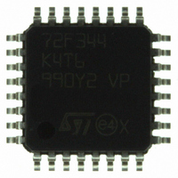
ST72F344K4T6 STMicroelectronics, ST72F344K4T6 Datasheet - Page 200

ST72F344K4T6
Manufacturer Part Number
ST72F344K4T6
Description
MCU 8BIT 16KB FLASH MEM 32-LQFP
Manufacturer
STMicroelectronics
Series
ST7r
Datasheet
1.ST72F344K2T6.pdf
(247 pages)
Specifications of ST72F344K4T6
Core Processor
ST7
Core Size
8-Bit
Speed
8MHz
Connectivity
I²C, LIN, SCI, SPI
Peripherals
LVD, POR, PWM, WDT
Number Of I /o
24
Program Memory Size
16KB (16K x 8)
Program Memory Type
FLASH
Eeprom Size
256 x 8
Ram Size
1K x 8
Voltage - Supply (vcc/vdd)
2.7 V ~ 5.5 V
Data Converters
A/D 12x10b
Oscillator Type
Internal
Operating Temperature
-40°C ~ 85°C
Package / Case
32-LQFP
Processor Series
ST72F3x
Core
ST7
Data Bus Width
8 bit
Data Ram Size
1 KB
Interface Type
I2C, SCI, SPI
Maximum Clock Frequency
8 MHz
Number Of Programmable I/os
34
Number Of Timers
2
Maximum Operating Temperature
+ 85 C
Mounting Style
SMD/SMT
Development Tools By Supplier
ST72F34X-SK/RAIS, ST7MDT40-EMU3, STX-RLINK
Minimum Operating Temperature
- 40 C
On-chip Adc
10 bit, 8 Channel
For Use With
497-5046 - KIT TOOL FOR ST7/UPSD/STR7 MCU
Lead Free Status / RoHS Status
Lead free / RoHS Compliant
Other names
497-5611
Available stocks
Company
Part Number
Manufacturer
Quantity
Price
Company:
Part Number:
ST72F344K4T6
Manufacturer:
STMicroelectronics
Quantity:
10 000
Company:
Part Number:
ST72F344K4T6TR
Manufacturer:
STMicroelectronics
Quantity:
10 000
- Current page: 200 of 247
- Download datasheet (3Mb)
Electrical characteristics
13.1.5
13.2
200/247
Pin input voltage
The input voltage measurement on a pin of the device is described in
Figure 86. Pin input voltage
Absolute maximum ratings
Stresses above those listed as “absolute maximum ratings” may cause permanent damage
to the device. This is a stress rating only and functional operation of the device under these
conditions is not implied. Exposure to maximum rating conditions for extended periods may
affect device reliability.
Table 84.
1. Directly connecting the RESET and I/O pins to V
2. I
|V
|V
V
V
Symbol
SSx
internal reset is generated or an unexpected change of the I/O configuration occurs (for example, due to a
corrupted program counter). To guarantee safe operation, this connection has to be done through a pull-up
or pull-down resistor (typical: 4.7 kΩ for RESET, 10 kΩ for I/Os). Unused I/O pins must be tied in the same
way to V
cannot be respected, the injection current must be limited externally to the I
injection is induced by V
pads, there is no positive injection current, and the corresponding V
DDx
ESD(HBM)
DD
INJ(PIN)
V
- V
- V
IN
- V
SS
DD
SS
must never be exceeded. This is implicitly insured if V
DD
|
| Variations between all the different ground pins
or V
Voltage characteristics
Supply voltage
Input voltage on any pin
Variations between different power pins
Electrostatic discharge voltage (human body
model)
SS
according to their reset configuration.
IN
>V
DD
while a negative injection is induced by V
Doc ID 12321 Rev 5
Ratings
V
IN
(1)&(2)
DD
or V
SS
ST7 PIN
could damage the device if an unintentional
IN
maximum is respected. If V
IN
maximum must always be respected
see
maximum ratings (electrical
sensitivity) on page 214
IN
V
<V
INJ(PIN)
Maximum value
SS
Section 13.8.3: Absolute
SS
-0.3 to V
ST72344xx ST72345xx
. For true open-drain
value. A positive
Figure
7.0
0.3
0.3
DD
IN
86.
+0.3
maximum
Unit
V
Related parts for ST72F344K4T6
Image
Part Number
Description
Manufacturer
Datasheet
Request
R

Part Number:
Description:
STMicroelectronics [RIPPLE-CARRY BINARY COUNTER/DIVIDERS]
Manufacturer:
STMicroelectronics
Datasheet:

Part Number:
Description:
STMicroelectronics [LIQUID-CRYSTAL DISPLAY DRIVERS]
Manufacturer:
STMicroelectronics
Datasheet:

Part Number:
Description:
BOARD EVAL FOR MEMS SENSORS
Manufacturer:
STMicroelectronics
Datasheet:

Part Number:
Description:
NPN TRANSISTOR POWER MODULE
Manufacturer:
STMicroelectronics
Datasheet:

Part Number:
Description:
TURBOSWITCH ULTRA-FAST HIGH VOLTAGE DIODE
Manufacturer:
STMicroelectronics
Datasheet:

Part Number:
Description:
Manufacturer:
STMicroelectronics
Datasheet:

Part Number:
Description:
DIODE / SCR MODULE
Manufacturer:
STMicroelectronics
Datasheet:

Part Number:
Description:
DIODE / SCR MODULE
Manufacturer:
STMicroelectronics
Datasheet:

Part Number:
Description:
Search -----> STE16N100
Manufacturer:
STMicroelectronics
Datasheet:

Part Number:
Description:
Search ---> STE53NA50
Manufacturer:
STMicroelectronics
Datasheet:

Part Number:
Description:
NPN Transistor Power Module
Manufacturer:
STMicroelectronics
Datasheet:

Part Number:
Description:
DIODE / SCR MODULE
Manufacturer:
STMicroelectronics
Datasheet:


