M38D59GCHP#U0 Renesas Electronics America, M38D59GCHP#U0 Datasheet - Page 125
M38D59GCHP#U0
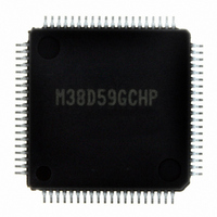
Manufacturer Part Number
M38D59GCHP#U0
Description
IC 740/38D5 MCU QZ-ROM 80LQFP
Manufacturer
Renesas Electronics America
Series
740/38000r
Datasheet
1.M38D58G8FPU0.pdf
(144 pages)
Specifications of M38D59GCHP#U0
Core Processor
740
Core Size
8-Bit
Speed
12.5MHz
Connectivity
SIO, UART/USART
Peripherals
LCD, LED, PWM, WDT
Number Of I /o
59
Program Memory Size
48KB (48K x 8)
Program Memory Type
QzROM
Ram Size
2K x 8
Voltage - Supply (vcc/vdd)
1.8 V ~ 5.5 V
Data Converters
A/D 8x10b
Oscillator Type
Internal
Operating Temperature
-20°C ~ 85°C
Package / Case
80-LQFP
Lead Free Status / RoHS Status
Lead free / RoHS Compliant
Eeprom Size
-
Available stocks
Company
Part Number
Manufacturer
Quantity
Price


38D5 Group
Rev.3.04
REJ03B0158-0304
3. JMP Instruction
When using the JMP instruction (indirect addressing mode), do
not specify the address where “FF
order 8 bits as the operand.
4. Multiplication and Division Instructions
(1) The MUL and DIV instructions are not affected by the T and
(2) Executing these instructions does not change the contents of
5. Read-Modify-Write Instruction
Do not execute any read-modify-write instruction to the read
invalid (address) SFR.
The read-modify-write instruction reads 1-byte of data from
memory, modifies the data, and writes 1-byte the data to the
original memory.
In the 740 Family, the read-modify-write instructions are the
following:
(1) Bit handling instructions:
(2) Shift and rotate instructions:
(3) Add and subtract instructions:
(4) Logical operation instructions (1’s complement):
Although not the read-modify-write instructions, add and
subtract/logical operation instructions (ADC, SBC, AND, EOR,
and ORA) when T flag = “1” operate in the way as the read-
modify-write instruction. Do not execute them to the read invalid
SFR.
<Reason>
When the read-modify-write instruction is executed to the read
invalid SFR, the following may result:
As reading is invalid, the read value is undefined. The instruction
modifies this undefined value and writes it back, so the written
value will be indeterminate.
D flags.
the processor status register.
CLB, SEB
ASL, LSR, ROL, ROR, RRF
DEC, INC
COM
May 20, 2008 Page 123 of 134
16
” is allocated to the low-
Notes on Peripheral Functions
Notes on I/O Ports
1. Use in Stand-By State
When using the MCU in stand-by state*
consumption, do not leave the input level of an I/O port
undefined. Be especially careful to the I/O ports for the N-
channel open-drain.
In this case, pull-up (connect to Vcc) or pull-down (connect to
Vss) these ports through a resistor.
When determining a resistance value, note the following:
When using a built-in pull-up resistor, note variations in current
values:
<Reason>
Even if a port is set to output by the direction register, when the
content of the port latch is “1”, the transistor becomes the OFF
state, which allows the port to be in the high-impedance state.
This may cause the level to be undefined depending on external
circuits.
As described above, if the input level of an I/O port is left
undefined, the power source current may flow because the
potential applied to the input buffer in the MCU will be unstable.
*
2. Modifying Output Data with Bit Handling Instruction
When the port latch of an I/O port is modified with the bit
handling instruction*
change.
<Reason>
I/O ports can be set to input mode or output mode in byte units.
When the port register is read or written, the following will be
operated:
• Port as input mode
• Port as output mode
Meanwhile, the bit handling instructions are the read-modify-
write instructions*
port register allows reading and writing a bit unspecified with the
instruction at the same time.
If an unspecified bit is set to input mode, the pin level is read and
the value is written to the port latch. At this time, if the original
content of the port latch and the pin level do not match, the
content of the port latch changes.
If an unspecified bit is set to output mode, the port latch is
normally read, but the peripheral function output is read in some
ports and the value is written to the port latch. At this time, if the
original content of the port latch and the peripheral function
output do not match, the content of the port latch changes.
*1 Bit handling instructions: CLB, SEB
*2 Read-modify-write instruction: Reads 1-byte of data from
1
Read: Read the pin level
Write: Write to the port latch
Read: Read the port latch or peripheral function output
Write: Write to the port latch (output the content of the port
Stand-by state: Stop mode by executing the STP instruction
• External circuit
• Variation in the output level during ordinary operation
• When setting as an input port: Fix the input level
• When setting as an output port: Prevent current from
memory, modifies the data, and writes 1-byte of the data to
the original memory.
flowing out externally.
latch from the pin)
(specifications vary depending on the port)
2
Wait mode by executing the WIT instruction
. Executing the bit handling instruction to the
1
, the value of an unspecified bit may
1
for low-power
Related parts for M38D59GCHP#U0
Image
Part Number
Description
Manufacturer
Datasheet
Request
R

Part Number:
Description:
KIT STARTER FOR M16C/29
Manufacturer:
Renesas Electronics America
Datasheet:

Part Number:
Description:
KIT STARTER FOR R8C/2D
Manufacturer:
Renesas Electronics America
Datasheet:

Part Number:
Description:
R0K33062P STARTER KIT
Manufacturer:
Renesas Electronics America
Datasheet:

Part Number:
Description:
KIT STARTER FOR R8C/23 E8A
Manufacturer:
Renesas Electronics America
Datasheet:

Part Number:
Description:
KIT STARTER FOR R8C/25
Manufacturer:
Renesas Electronics America
Datasheet:

Part Number:
Description:
KIT STARTER H8S2456 SHARPE DSPLY
Manufacturer:
Renesas Electronics America
Datasheet:

Part Number:
Description:
KIT STARTER FOR R8C38C
Manufacturer:
Renesas Electronics America
Datasheet:

Part Number:
Description:
KIT STARTER FOR R8C35C
Manufacturer:
Renesas Electronics America
Datasheet:

Part Number:
Description:
KIT STARTER FOR R8CL3AC+LCD APPS
Manufacturer:
Renesas Electronics America
Datasheet:
Part Number:
Description:
KIT STARTER FOR RX610
Manufacturer:
Renesas Electronics America
Datasheet:

Part Number:
Description:
KIT STARTER FOR R32C/118
Manufacturer:
Renesas Electronics America
Datasheet:

Part Number:
Description:
KIT DEV RSK-R8C/26-29
Manufacturer:
Renesas Electronics America
Datasheet:

Part Number:
Description:
KIT STARTER FOR SH7124
Manufacturer:
Renesas Electronics America
Datasheet:

Part Number:
Description:
KIT STARTER FOR H8SX/1622
Manufacturer:
Renesas Electronics America
Datasheet:

Part Number:
Description:
KIT DEV FOR SH7203
Manufacturer:
Renesas Electronics America
Datasheet: