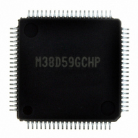
M38D59GCHP#U0 Renesas Electronics America, M38D59GCHP#U0 Datasheet - Page 85

M38D59GCHP#U0
Manufacturer Part Number
M38D59GCHP#U0
Description
IC 740/38D5 MCU QZ-ROM 80LQFP
Manufacturer
Renesas Electronics America
Series
740/38000r
Datasheet
1.M38D58G8FPU0.pdf
(144 pages)
Specifications of M38D59GCHP#U0
Core Processor
740
Core Size
8-Bit
Speed
12.5MHz
Connectivity
SIO, UART/USART
Peripherals
LCD, LED, PWM, WDT
Number Of I /o
59
Program Memory Size
48KB (48K x 8)
Program Memory Type
QzROM
Ram Size
2K x 8
Voltage - Supply (vcc/vdd)
1.8 V ~ 5.5 V
Data Converters
A/D 8x10b
Oscillator Type
Internal
Operating Temperature
-20°C ~ 85°C
Package / Case
80-LQFP
Lead Free Status / RoHS Status
Lead free / RoHS Compliant
Eeprom Size
-
Available stocks
Company
Part Number
Manufacturer
Quantity
Price
38D5 Group
Rev.3.04
REJ03B0158-0304
Functions To Inhibit Rewriting Flash Memory Version
To prevent the contents of internal flash memory from being read
out or rewritten easily, this MCU incorporates a ROM code
protect function for use in parallel I/O mode and an ID code
check function for use in standard serial I/O mode.
• ROM Code Protect Function
The ROM code protect function is the function to inhibit reading
out or modifying the contents of internal flash memory by using
the ROM code protect control address (address FFDB
parallel I/O mode. Figure 78 shows the ROM code protect
control address (address FFDB
User ROM area.)
Fig 78. Structure of ROM code protect control address
May 20, 2008 Page 83 of 134
b7
Notes 1: When ROM code protect is turned on, the internal flash memory is protected
2: When ROM code protect level 2 is turned on, ROM code readout by a shipment
3: The ROM code protect reset bits can be used to turn off ROM code protect level
against readout or modification in parallel I/O mode.
inspection LSI tester, etc. also is inhibited.
1 and ROM code protect level 2.
However, no change can be made in parallel I/O mode. Use serial I/O mode or
other modes to change settings.
16
). (This address exists in the
1
b0
1
ROM code protect control address (address FFDB
ROMCP (FF
Reserved bits (“1” at read/write)
ROM code protect level 2 set bits (ROMCP2)
ROM code protect reset bits (ROMCR)
ROM code protect level 1 set bits (ROMCP1)
b3b2
0 0: Protect enabled
0 1: Protect enabled
1 0: Protect enabled
1 1: Protect disabled
b5b4
0 0: Protect removed
0 1: Protect set bits effective
1 0: Protect set bits effective
1 1: Protect set bits effective
b7b6
0 0: Protect enabled
0 1: Protect enabled
1 0: Protect enabled
1 1: Protect disabled
16
) in
16
when shipped)
If one or both of the pair of ROM code protect bits is set to “0”,
the ROM code protect is turned on, so that the contents of
internal flash memory are protected against readout and
modification. The ROM code protect is implemented in two
levels. If level 2 is selected, the flash memory is protected even
against readout by a shipment inspection LSI tester, etc. When an
attempt is made to select both level 1 and level 2, level 2 is
selected by default.
If both of the two ROM code protect reset bits are set to “00”, the
ROM code protect is turned off, so that the contents of internal
flash memory can be readout or modified. Once the ROM code
protect is turned on, the contents of the ROM code protect reset
bits cannot be modified in parallel I/O mode. Use standard serial
I/O mode or other modes to rewrite the contents of the ROM
code protect disable bits.
Rewriting of only the ROM code protect control address (address
FFDB
protect reset bit, rewrite the whole user ROM area (block 0)
containing the ROM code protect control address.
16
) cannot be performed. When rewriting the ROM code
(3)
(1, 2)
(1)
16
)


