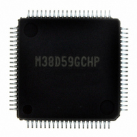
M38D59GCHP#U0 Renesas Electronics America, M38D59GCHP#U0 Datasheet - Page 130

M38D59GCHP#U0
Manufacturer Part Number
M38D59GCHP#U0
Description
IC 740/38D5 MCU QZ-ROM 80LQFP
Manufacturer
Renesas Electronics America
Series
740/38000r
Datasheet
1.M38D58G8FPU0.pdf
(144 pages)
Specifications of M38D59GCHP#U0
Core Processor
740
Core Size
8-Bit
Speed
12.5MHz
Connectivity
SIO, UART/USART
Peripherals
LCD, LED, PWM, WDT
Number Of I /o
59
Program Memory Size
48KB (48K x 8)
Program Memory Type
QzROM
Ram Size
2K x 8
Voltage - Supply (vcc/vdd)
1.8 V ~ 5.5 V
Data Converters
A/D 8x10b
Oscillator Type
Internal
Operating Temperature
-20°C ~ 85°C
Package / Case
80-LQFP
Lead Free Status / RoHS Status
Lead free / RoHS Compliant
Eeprom Size
-
Available stocks
Company
Part Number
Manufacturer
Quantity
Price
38D5 Group
Rev.3.04
REJ03B0158-0304
Notes on Serial I/O1
1. Write to Baud Rate Generator
Write to the baud rate generator while transmission/reception is
stopped.
2. Setting Sequence When Serial I/O1 Transmit
To use the serial I/O1 transmit interrupt, if the interrupt
occurrence synchronized with settings is not required, take the
following sequence:
(1) Set the serial I/O1 transmit interrupt enable bit (bit 2 of
(2) Set the transmit enable bit to “1”.
(3) After one or more instructions have been executed, set the
(4) Set the serial I/O1 transmit interrupt enable bit to “1”
<Reason>
When the transmit enable bit is set to “1”, the transmit buffer
empty flag (bit 0 of serial I/O1 status register) and the transmit
shift completion flag are set to “1”.
This allows an interrupt request to be generated regardless of
which interrupt occurrence source has been selected by the
transmit interrupt source selection bit (bit 3 of serial I/O1 control
register) and the serial I/O1 transmit interrupt request bit is set to
“1”.
3. Data Transmission Control Using Transmit Shift
After transmit data is written to the transmit buffer register, the
transmit shift completion flag (bit 2 of serial I/O1 status register
(address 0019
1.5 cycles of the system clock. Thus, after transmit data is written
to the transmit buffer register, note this delay when controlling
data transmission by referencing the transmit shift completion
flag.
4. Setting Serial I/O1 Control Register
Before setting the serial I/O1 control register again, first set both
the transmit enable bit and the receive enable bit to “0” and
initialize the transmission and reception circuits.
Fig. 104 Sequence of setting serial I/O1 control register
5. Pin Status After Transmission Completed
After transmission is completed, the TxD pin retains the level
when transmission is completed.
When the internal clock is selected in clock synchronous serial
I/O mode, the S
Set both the transmit enable bit (TE) and the receive
enable bit (RE), or one of them to “1”.
Set both the transmit enable bit (TE) and the
receive enable bit (RE) to “0”
Set bits 0 to 3, and 6 of the serial I/O1 control
register.
Interrupt Used
Completion Flag
interrupt control register 2 (address 003F
(disabled).
serial I/O1 transmit interrupt request bit (bit 2 of interrupt
request register 2 (address 003D
(enabled).
16
May 20, 2008 Page 128 of 134
)) changes from “1” to “0” after a delay of 0.5 to
CLK1
pin is set to “H”.
16
)) to “0” (no interrupt).
Settings can be made with
the LDM instruction at the
same time
16
)) to “0”
6. Serial I/O1 Enable Bit during Transmit Operation
During transmission, if the serial I/O1 enable bit (bit 7 of serial
I/O1 control register (address 001A
function is set to an I/O port and the internal transmit operation
continues even though transmit data is not output externally.
Also, if the transmit buffer register is written in this state,
transmit operation starts internally. If the serial I/O1 enable bit is
set to “1” at this time, transmit data is output to the TxD pin from
that point.
7. Transmission
During data transmission, if the external clock is selected as the
synchronous clock, set the transmit enable bit to “1” while S
is set to “H”. Also, write to the transmit buffer register while
S
8. Receive Operation in Clock Synchronous Serial I/O
During reception in clock synchronous serial I/O mode, set both
the transmit enable bit and the receive enable bit to “1”. Then
write dummy data to the transmit buffer register. When the
internal clock is selected as the synchronous clock, the
synchronous clock is output at this point and receive operation
starts. When the external clock is selected, reception is enabled at
this point and inputting the external clock starts transmit
operation.
The P4
buffer register.
9. Transmit/Receive Operation in Clock Synchronous
In clock synchronous serial I/O mode, set the transmit enable bit
and the receive enable bit to “0” simultaneously to stop
transmit/receive operations. If only one of the operations is
stopped, transmission and reception cannot be synchronized,
which will cause a bit error.
Notes on Serial I/O2
1. Switching Synchronous Clock
If the synchronous clock is switched by the serial I/O2
synchronous clock selection bit (bit 6 of serial I/O2 control
register (address 001D
(writing to serial I/O2 register (address 001F
2. Notes When External Clock Selected
When the external clock is selected as the synchronous clock, the
S
However, if the synchronous clock is continuously input, the
serial I/O2 register continues shifting and the S
outputting transmit data.
Also, write to the serial I/O2 register while S
When the internal clock is selected as the synchronous clock, the
S
completed.
CLK1
OUT2
OUT2
Selected
Mode
Serial I/O Mode
is set to “H”.
pin retains the D
pin is placed in the high-impedance state after transfer is
1
/TxD pin outputs dummy data written in the transmit
Control
7
16
level after transfer is completed.
)), initialize the serial I/O2 counter
When
16
)) is set to “0”, the pin
16
CLK2
External
)).
OUT2
is set to “H”.
pin keeps
Clock
CLK1


