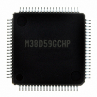
M38D59GCHP#U0 Renesas Electronics America, M38D59GCHP#U0 Datasheet - Page 30

M38D59GCHP#U0
Manufacturer Part Number
M38D59GCHP#U0
Description
IC 740/38D5 MCU QZ-ROM 80LQFP
Manufacturer
Renesas Electronics America
Series
740/38000r
Datasheet
1.M38D58G8FPU0.pdf
(144 pages)
Specifications of M38D59GCHP#U0
Core Processor
740
Core Size
8-Bit
Speed
12.5MHz
Connectivity
SIO, UART/USART
Peripherals
LCD, LED, PWM, WDT
Number Of I /o
59
Program Memory Size
48KB (48K x 8)
Program Memory Type
QzROM
Ram Size
2K x 8
Voltage - Supply (vcc/vdd)
1.8 V ~ 5.5 V
Data Converters
A/D 8x10b
Oscillator Type
Internal
Operating Temperature
-20°C ~ 85°C
Package / Case
80-LQFP
Lead Free Status / RoHS Status
Lead free / RoHS Compliant
Eeprom Size
-
Available stocks
Company
Part Number
Manufacturer
Quantity
Price
38D5 Group
Rev.3.04
REJ03B0158-0304
INTERRUPTS
The 38D5 Group interrupts are vector interrupts with a fixed
priority scheme, and generated by 16 sources among 17 sources:
6 external, 10 internal, and 1 software.
The interrupt sources, vector addresses
are shown in Table 11.
Each interrupt except the BRK instruction interrupt has the
interrupt request bit and the interrupt enable bit. These bits and
the interrupt disable flag (I flag) control the acceptance of
interrupt requests. Figure 18 shows an interrupt control diagram.
Table 11 Interrupt vector addresses and priority
NOTES:
Reset
INT
INT
INT
INT
INT
Key input
(key-on wakeup)
Timer X
Timer 1
Timer 2
Timer 3
Timer 4
Serial I/O1 receive
Serial I/O1 transmit
Serial I/O2
CNTR
Timer Y
CNTR
A/D conversion
BRK instruction
1. Vector addresses contain interrupt jump destination addresses.
2. Reset function in the same way as an interrupt with the highest priority.
3. INT
Interrupt Source
0
01
1
11
2
(INT
(INT
)
)
(2)
(3)
0
1
(3)
0
, and INT
10
00
or
or
May 20, 2008 Page 28 of 134
1
input pins are selected by the interrupt edge selection register (INTEDGE).
Priority
10
12
13
14
15
16
17
11
1
2
3
4
5
6
7
8
9
Vector Addresses
FFDD
FFFD
FFFB
FFEF
FFED
FFEB
FFDF
FFF9
FFF7
FFF5
FFF3
FFF1
FFE9
FFE7
FFE5
FFE3
FFE1
High
16
16
16
16
16
16
16
16
16
16
16
16
16
16
16
16
16
(1)
, and interrupt priority
FFDC
FFFC
FFEE
FFEC
FFEA
FFDE
FFFA
FFF8
FFF6
FFF4
FFF2
FFF0
FFE8
FFE6
FFE4
FFE2
FFE0
Low
16
16
16
16
16
16
16
16
16
16
16
16
16
16
16
16
16
(1)
At reset
At detection of either rising or falling
edge of INT
At detection of either rising or falling
edge of INT
At detection of either rising or falling
edge of INT
At falling of ports P2
input logical level AND
At timer X underflow
At timer 1 underflow
At timer 2 underflow
At timer 3 underflow
At timer 4 underflow
At completion of serial I/O1 data receive Valid only when serial I/O1 is selected
At completion of serial I/O1 transmit
shift or transmit buffer is empty
At completion of serial I/O2 data
transmit/receive
At detection of either rising or falling
edge of CNTR
At timer Y underflow
At detection of either rising or falling
edge of CNTR
At completion of A/D conversion
At BRK instruction execution
Generating Conditions
Interrupt Request
0
1
2
input
input
input
0
1
input
input
An interrupt requests is accepted when all of the following
conditions are satisfied:
Though the interrupt priority is determined by hardware, priority
processing can be performed by software using the above bits
and flag.
0
• Interrupt disable flag ................................ “0”
• Interrupt request bit .................................. “1”
• Interrupt enable bit ................................... “1”
−P2
3,
P4
4
−P4
7
Non-maskable
External interrupt (active edge selectable)
External interrupt (active edge selectable)
Valid when INT
External interrupt (active edge selectable)
Valid when Key input interrupt is
selected External interrupt (falling valid)
Valid only when serial I/O1 is selected
External interrupt (active edge selectable)
External interrupt (active edge selectable)
Non-maskable software interrupt
2
Remarks
interrupt is selected


