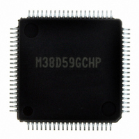
M38D59GCHP#U0 Renesas Electronics America, M38D59GCHP#U0 Datasheet - Page 29

M38D59GCHP#U0
Manufacturer Part Number
M38D59GCHP#U0
Description
IC 740/38D5 MCU QZ-ROM 80LQFP
Manufacturer
Renesas Electronics America
Series
740/38000r
Datasheet
1.M38D58G8FPU0.pdf
(144 pages)
Specifications of M38D59GCHP#U0
Core Processor
740
Core Size
8-Bit
Speed
12.5MHz
Connectivity
SIO, UART/USART
Peripherals
LCD, LED, PWM, WDT
Number Of I /o
59
Program Memory Size
48KB (48K x 8)
Program Memory Type
QzROM
Ram Size
2K x 8
Voltage - Supply (vcc/vdd)
1.8 V ~ 5.5 V
Data Converters
A/D 8x10b
Oscillator Type
Internal
Operating Temperature
-20°C ~ 85°C
Package / Case
80-LQFP
Lead Free Status / RoHS Status
Lead free / RoHS Compliant
Eeprom Size
-
Available stocks
Company
Part Number
Manufacturer
Quantity
Price
38D5 Group
Rev.3.04
REJ03B0158-0304
Table 10 Termination of unused pins
P0
P1
P2
P2
P3
P4
P4
P4
P4
P4
P4
P4
P4
P5
P5
P5
P5
P6
P6
P6
P6
P6
P6
P6
(LED
P6
P7
P7
P7
P7
P7
V
V
V
COM
COM
COM
V
X
X
L3
L2
L1
REF
IN
OUT
0
0
0
2
0
7
0
1
2
3
4
5
6
7
0
1
2
7
0
1
2
3
4
5
6
7
0
1
3
4
/SEG
/SEG
/SEG
/T
/SEG
/SEG
/R
/T
/S
/S
/S
/S
/S
/S
/AN
/AN
/AN
/AN
/X
/X
/INT
/T
/INT
/T
/INT
/CNTR
/C
/C
/PWM
/PWM
4
0
4
7
2OUT
X
XOUT2
XOUT1
CLK1
RDY1
IN2
OUT2
CLK2
RDY2
CIN
COUT
X
)
1
2
−COM
/SEG
/SEG
D
/INT
/INT
D
0
1
2
7
8
16
24
00
2
10
Pin
−P0
/(KW
/RTP
/RTP
−P5
/ADKEY
/(LED
0
7
−P1
−P3
/CKOUT
/(LED
/CNTR
0
1
/(KW
/(KW
/(KW
/(KW
1
/T
/T
01
11
/(LED
/(LED
/(LED
35
32
7
6
/SEG
7
7
3
3OUT
4OUT
/AN
/SEG
/SEG
0
0
1
−
May 20, 2008 Page 27 of 134
)
2
4
2
1
3
0
)
)−
)
)
)
0
)
0
6
1
3
15
5
/
23
31
)
)
)
I/O port
Disable the voltage multiplier, and
connect to V
I/O port
Set the V
apply a Vcc level voltage to V
V
Connect to V
Open
Open
Connect to V
When only on-chip oscillator is used,
connect to V
When external clock is input or when
only on-chip oscillator is used, open.
L3 ≥
V
L2 ≥
L3
Termination 1
V
connect bit to “1” and
CC
L1
SS
SS
CC
through a resistor.
through a resistor.
L3
pin.
When selecting SEG output, open.
When selecting RxD function, perform
termination of input port.
When selecting TxD function, perform
termination of output port.
When selecting external clock input,
perform termination of input port.
When selecting S
termination of output port.
When selecting S
termination of input port.
When selecting S
termination of output port.
When selecting external clock input,
perform termination of output port.
When selecting S
termination of output port.
When selecting AN function, these pins
can be opened. (A/D conversion result
cannot be guaranteed.)
Do not select X
function by program.
When selecting INT function,
perform termination of input port.
When selecting T
termination of output port.
When selecting INT function,
perform termination of input port.
When selecting T
termination of output port.
When selecting CNTR input function or INT
function, perform termination of input port.
When selecting CNTR input function,
perform termination of input port.
When selecting INT function, disable the voltage
multiplier, and connect to V
When selecting T
function, perform termination of output port.
When selecting PWM, T
function, perform termination of output port.
Set the V
V
L3
pin open.
L3
connect bit to “0” and leave the
Termination 2
CIN
XOUT
XOUT
2OUT
RDY1
IN2
OUT2
RDY2
−X
function, perform
−
−
−
−
−
−
−
COUT
function, perform
function, perform
function, perform
function or CKOUT
function, perform
function, perform
SS
3OUT
oscillation
through a resistor.
, or T
4OUT
When selecting internal clock output,
perform termination of output port.
When selecting internal clock output,
perform termination of output port.
When selecting RTP function,
perform termination of output port.
When selecting ADKEY function,
pull-up this pin through a resistor.
Termination 3
−
−
−
−
−
−
−
−
−
−
−
−
−
−
−
−
−
−
−
−
−
−
−
−
−
−


