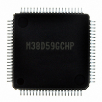
M38D59GCHP#U0 Renesas Electronics America, M38D59GCHP#U0 Datasheet - Page 44

M38D59GCHP#U0
Manufacturer Part Number
M38D59GCHP#U0
Description
IC 740/38D5 MCU QZ-ROM 80LQFP
Manufacturer
Renesas Electronics America
Series
740/38000r
Datasheet
1.M38D58G8FPU0.pdf
(144 pages)
Specifications of M38D59GCHP#U0
Core Processor
740
Core Size
8-Bit
Speed
12.5MHz
Connectivity
SIO, UART/USART
Peripherals
LCD, LED, PWM, WDT
Number Of I /o
59
Program Memory Size
48KB (48K x 8)
Program Memory Type
QzROM
Ram Size
2K x 8
Voltage - Supply (vcc/vdd)
1.8 V ~ 5.5 V
Data Converters
A/D 8x10b
Oscillator Type
Internal
Operating Temperature
-20°C ~ 85°C
Package / Case
80-LQFP
Lead Free Status / RoHS Status
Lead free / RoHS Compliant
Eeprom Size
-
Available stocks
Company
Part Number
Manufacturer
Quantity
Price
38D5 Group
Rev.3.04
REJ03B0158-0304
Fig. 31 Block diagram of Timer Y
• Timer Y
Timer Y is a 16-bit timer. The timer Y count source can be
selected by setting the timer Y mode register. X
selected as the count source. When X
source, counting can be performed regardless of X
or on-chip oscillator oscillation.
Four operating modes can be selected for timer Y by the timer Y
mode register. Also, the real time port can be controlled.
(1) Timer Mode
The timer Y count source can be selected by setting the timer Y
mode register.
(2) Period Measurement Mode
The interrupt request is generated at rising or falling edge of
CNTR
latch is reloaded in timer Y and timer Y continues counting.
Except for that, this mode operates just as in the timer mode.
The timer value just before the reloading at rising or falling of
CNTR
the reload.
The rising or falling timing of CNTR
CNTR
CNTR
φSOURCE
P5
P5
1
1
1
1
1
0
pin to input mode.
/RTP
pin input is retained until the timer Y is read once after
interrupt. When using this mode, set the port sharing the
pin input signal. Simultaneously, the value in timer Y
/RTP
(1)
Xc
1
CNTR
0
Frequency divider
/AN
/AN
May 20, 2008 Page 42 of 134
IN
1
0
1
Count source selection bit
P5
register
P5
register
1
0
“0”
“1”
direction
direction
Real time port 1
control bit
CNTR
edge switch bit
Real time port 2
control bit
2
Timer Y dividing frequency selection bit
“1”
“0”
1
active
“0”
“1”
“0”
“1”
P5
P5
1
CIN
0
latch
“10”
latch
1
“00”, “01”, “11”
is selected as the count
pin input is found by
Latch
Latch
Timer Y operating
mode bits
Q D
Q D
Timer Y count
stop bit
IN
Note1: φSOURCE indicates the followings:
Timer Y write control bit
CIN
oscillation
RTP
time port
RTP
time port
•X
•On-chip oscillator divided by 4 in the on-chip oscillator mode
•Sub-clock in the low-speed mode
can be
IN
Timer Y (low-order) latch (8) Timer Y (high-order) latch (8)
1
0
input in the frequency/2, 4, or 8 mode
data for real
Timer Y (low-order)(8)
data for real
Rising edge detection
Falling edge detection
(3) Event Counter Mode
The timer counts signals input through the CNTR
Except for that, this mode operates just as in the timer mode.
When using this mode, set the port sharing the CNTR
input mode.
(4) Pulse Width HL Continuously Measurement Mode
The interrupt request is generated at both rising and falling edges
of CNTR
just as in the period measurement mode. When using this mode,
set the port sharing the CNTR
(5) Real Time Port Control
When the real time port function is valid, data for the real time
port is output from ports P5
underflows.(However, if the real time port control bit is changed
from “0” to “1” after the data for real time port is set, data is
output independent of the timer Y operation.) When the data for
the real time port is changed while the real time port function is
valid, the changed data is output at the next underflow of timer
Y. Before using this function, set the P5
registers to output.
Real time port 1 control bit
Real time port 2 control bit
1
pin input signal. Except for that, this mode operates
Timer Y (high-order)(8)
Pulse width HL continuous
measurement mode
Period measurement
mode
“0”
“1”
“0”
“1”
Timer Y operating mode bits
Timer Y mode register
write signal
Timer Y mode register
write signal
1
0
“00”, “01”, “10”
pin to input mode.
and P5
“11”
1
0
each time the timer Y
and P5
Data bus
1
1
Timer Y
interrupt request
CNTR
interrupt request
pin.
port direction
1
1
pin to


