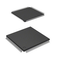
DF2161BVTE10 Renesas Electronics America, DF2161BVTE10 Datasheet - Page 44

DF2161BVTE10
Manufacturer Part Number
DF2161BVTE10
Description
MCU 3V 128K 144-TQFP
Manufacturer
Renesas Electronics America
Series
H8® H8S/2100r
Datasheet
1.DF2160BVT10V.pdf
(847 pages)
Specifications of DF2161BVTE10
Core Processor
H8S/2000
Core Size
16-Bit
Speed
10MHz
Connectivity
Host Interface (LPC), I²C, IrDA, SCI, X-Bus
Peripherals
PWM, WDT
Number Of I /o
114
Program Memory Size
128KB (128K x 8)
Program Memory Type
FLASH
Ram Size
4K x 8
Voltage - Supply (vcc/vdd)
2.7 V ~ 3.6 V
Data Converters
A/D 8x10b; D/A 2x8b
Oscillator Type
Internal
Operating Temperature
-20°C ~ 75°C
Package / Case
144-TQFP, 144-VQFP
Lead Free Status / RoHS Status
Contains lead / RoHS non-compliant
Eeprom Size
-
Other names
HD64F2161BVTE10
HD64F2161BVTE10
HD64F2161BVTE10
- Current page: 44 of 847
- Download datasheet (5Mb)
Figure 14.5
Figure 14.6
Figure 14.7
Figure 14.8
Section 15 Serial Communication Interface (SCI and IrDA)
Figure 15.1
Figure 15.2
Figure 15.3
Figure 15.4
Figure 15.5
Figure 15.6
Figure 15.7
Figure 15.8
Figure 15.9
Figure 15.9
Figure 15.10 Example of Communication Using Multiprocessor Format
Figure 15.11 Sample Multiprocessor Serial Transmission Flowchart....................................... 389
Figure 15.12 Example of SCI Receive Operation (Example with 8-Bit Data,
Figure 15.13 Sample Multiprocessor Serial Reception Flowchart (1) ...................................... 391
Figure 15.13 Sample Multiprocessor Serial Reception Flowchart (2) ...................................... 392
Figure 15.14 Data Format in Clocked Synchronous Communication (LSB-First) ................... 393
Figure 15.15 Sample SCI Initialization Flowchart.................................................................... 394
Figure 15.16 Example of SCI Transmit Operation in Clocked Synchronous Mode ................. 396
Figure 15.17 Sample Serial Transmission Flowchart................................................................ 397
Figure 15.18 Example of SCI Receive Operation in Clocked Synchronous Mode................... 398
Figure 15.19 Sample Serial Reception Flowchart ..................................................................... 399
Figure 15.20 Sample Flowchart of Simultaneous Serial Transmission and Reception ............. 401
Figure 15.21 IrDA Block Diagram............................................................................................ 402
Figure 15.22 IrDA Transmission and Reception....................................................................... 403
Figure 15.23 Example of Transmission Using DTC in Clocked Synchronous Mode............... 407
Figure 15.24 Sample Flowchart for Mode Transition during Transmission ............................. 408
Figure 15.25 Pin States during Transmission in Asynchronous Mode (Internal Clock) ........... 409
Figure 15.26 Pin States during Transmission in Clocked Synchronous Mode
Rev. 3.00 Mar 21, 2006 page xlii of liv
Output Timing of RESO signal............................................................................ 355
Writing to TCNT and TCSR (WDT_0) ............................................................... 356
Conflict between TCNT Write and Increment..................................................... 357
Sample Circuit for Resetting System by RESO Signal........................................ 358
Block Diagram of SCI ......................................................................................... 360
Data Format in Asynchronous Communication
(Example with 8-Bit Data, Parity, Two Stop Bits) .............................................. 376
Receive Data Sampling Timing in Asynchronous Mode..................................... 378
Relation between Output Clock and Transmit Data Phase
(Asynchronous Mode) ......................................................................................... 379
Sample SCI Initialization Flowchart.................................................................... 380
Example of SCI Transmit Operation in Asynchronous Mode
(Example with 8-Bit Data, Parity, One Stop Bit)................................................. 381
Sample Serial Transmission Flowchart................................................................ 382
Example of SCI Receive Operation in Asynchronous Mode
(Example with 8-Bit Data, Parity, One Stop Bit)................................................. 383
Sample Serial Reception Flowchart (1) ............................................................... 385
Sample Serial Reception Flowchart (2) ............................................................... 386
(Transmission of Data H'AA to Receiving Station A)......................................... 388
Multiprocessor Bit, One Stop Bit) ....................................................................... 390
(Internal Clock).................................................................................................... 409
Related parts for DF2161BVTE10
Image
Part Number
Description
Manufacturer
Datasheet
Request
R

Part Number:
Description:
KIT STARTER FOR M16C/29
Manufacturer:
Renesas Electronics America
Datasheet:

Part Number:
Description:
KIT STARTER FOR R8C/2D
Manufacturer:
Renesas Electronics America
Datasheet:

Part Number:
Description:
R0K33062P STARTER KIT
Manufacturer:
Renesas Electronics America
Datasheet:

Part Number:
Description:
KIT STARTER FOR R8C/23 E8A
Manufacturer:
Renesas Electronics America
Datasheet:

Part Number:
Description:
KIT STARTER FOR R8C/25
Manufacturer:
Renesas Electronics America
Datasheet:

Part Number:
Description:
KIT STARTER H8S2456 SHARPE DSPLY
Manufacturer:
Renesas Electronics America
Datasheet:

Part Number:
Description:
KIT STARTER FOR R8C38C
Manufacturer:
Renesas Electronics America
Datasheet:

Part Number:
Description:
KIT STARTER FOR R8C35C
Manufacturer:
Renesas Electronics America
Datasheet:

Part Number:
Description:
KIT STARTER FOR R8CL3AC+LCD APPS
Manufacturer:
Renesas Electronics America
Datasheet:

Part Number:
Description:
KIT STARTER FOR RX610
Manufacturer:
Renesas Electronics America
Datasheet:

Part Number:
Description:
KIT STARTER FOR R32C/118
Manufacturer:
Renesas Electronics America
Datasheet:

Part Number:
Description:
KIT DEV RSK-R8C/26-29
Manufacturer:
Renesas Electronics America
Datasheet:

Part Number:
Description:
KIT STARTER FOR SH7124
Manufacturer:
Renesas Electronics America
Datasheet:

Part Number:
Description:
KIT STARTER FOR H8SX/1622
Manufacturer:
Renesas Electronics America
Datasheet:

Part Number:
Description:
KIT DEV FOR SH7203
Manufacturer:
Renesas Electronics America
Datasheet:


