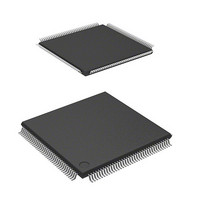
DF2161BVTE10 Renesas Electronics America, DF2161BVTE10 Datasheet - Page 667

DF2161BVTE10
Manufacturer Part Number
DF2161BVTE10
Description
MCU 3V 128K 144-TQFP
Manufacturer
Renesas Electronics America
Series
H8® H8S/2100r
Datasheet
1.DF2160BVT10V.pdf
(847 pages)
Specifications of DF2161BVTE10
Core Processor
H8S/2000
Core Size
16-Bit
Speed
10MHz
Connectivity
Host Interface (LPC), I²C, IrDA, SCI, X-Bus
Peripherals
PWM, WDT
Number Of I /o
114
Program Memory Size
128KB (128K x 8)
Program Memory Type
FLASH
Ram Size
4K x 8
Voltage - Supply (vcc/vdd)
2.7 V ~ 3.6 V
Data Converters
A/D 8x10b; D/A 2x8b
Oscillator Type
Internal
Operating Temperature
-20°C ~ 75°C
Package / Case
144-TQFP, 144-VQFP
Lead Free Status / RoHS Status
Contains lead / RoHS non-compliant
Eeprom Size
-
Other names
HD64F2161BVTE10
HD64F2161BVTE10
HD64F2161BVTE10
- Current page: 667 of 847
- Download datasheet (5Mb)
23.4
The flash memory is controlled by means of the pins shown in table 23.2.
Table 23.2 Pin Configuration
23.5
The flash memory has the following registers. To access FLMCR1, FLMCR2, EBR1, or EBR2,
the FLSHE bit in the serial/timer control register (STCR) should be set to 1. For details on the
serial/timer control register, refer to section 3.2.3, Serial Timer Control Register (STCR).
23.5.1
FLMCR1, used together with FLMCR2, makes the flash memory transit to program mode,
program-verify mode, erase mode, or erase-verify mode. For details on register setting, refer to
section 23.8, Flash Memory Programming/Erasing.
FLMCR1 is initialized to H'80 by a reset, or in hardware standby mode, software standby mode,
sub-active mode, sub-sleep mode, or watch mode.
Pin Name
RES
MD1
MD0
P92
P91
P90
TxD1
RxD1
Flash memory control register 1 (FLMCR1)
Flash memory control register 2 (FLMCR2)
Erase block register 1 (EBR1)
Erase block register 2 (EBR2)
Register Descriptions
Flash Memory Control Register 1 (FLMCR1)
Input/Output Pins
I/O
Input
Input
Input
Input
Input
Input
Output
Input
Function
Reset
Sets this LSI’s operating mode
Sets this LSI’s operating mode
Sets this LSI’s operating mode
Sets this LSI’s operating mode
Sets this LSI’s operating mode
Serial transmit data output
Serial receive data input
Rev. 3.00 Mar 21, 2006 page 611 of 788
REJ09B0300-0300
Section 23 ROM
Related parts for DF2161BVTE10
Image
Part Number
Description
Manufacturer
Datasheet
Request
R

Part Number:
Description:
KIT STARTER FOR M16C/29
Manufacturer:
Renesas Electronics America
Datasheet:

Part Number:
Description:
KIT STARTER FOR R8C/2D
Manufacturer:
Renesas Electronics America
Datasheet:

Part Number:
Description:
R0K33062P STARTER KIT
Manufacturer:
Renesas Electronics America
Datasheet:

Part Number:
Description:
KIT STARTER FOR R8C/23 E8A
Manufacturer:
Renesas Electronics America
Datasheet:

Part Number:
Description:
KIT STARTER FOR R8C/25
Manufacturer:
Renesas Electronics America
Datasheet:

Part Number:
Description:
KIT STARTER H8S2456 SHARPE DSPLY
Manufacturer:
Renesas Electronics America
Datasheet:

Part Number:
Description:
KIT STARTER FOR R8C38C
Manufacturer:
Renesas Electronics America
Datasheet:

Part Number:
Description:
KIT STARTER FOR R8C35C
Manufacturer:
Renesas Electronics America
Datasheet:

Part Number:
Description:
KIT STARTER FOR R8CL3AC+LCD APPS
Manufacturer:
Renesas Electronics America
Datasheet:

Part Number:
Description:
KIT STARTER FOR RX610
Manufacturer:
Renesas Electronics America
Datasheet:

Part Number:
Description:
KIT STARTER FOR R32C/118
Manufacturer:
Renesas Electronics America
Datasheet:

Part Number:
Description:
KIT DEV RSK-R8C/26-29
Manufacturer:
Renesas Electronics America
Datasheet:

Part Number:
Description:
KIT STARTER FOR SH7124
Manufacturer:
Renesas Electronics America
Datasheet:

Part Number:
Description:
KIT STARTER FOR H8SX/1622
Manufacturer:
Renesas Electronics America
Datasheet:

Part Number:
Description:
KIT DEV FOR SH7203
Manufacturer:
Renesas Electronics America
Datasheet:


